FMM-less OLED Patterning Patents
Drawing OLED pixels color by color without an FMM comes down to two questions: whether the unwanted organics are peeled away with a mold (lift-off) or etched from above, and whether an overhang cutting the pixels apart stays in the panel. If it stays, it also cuts a common cathode laid later, so the overhang method reads as laying the cathode color by color and connecting it through the overhang. The principles were first written down not by panel makers but by a US university and startup, an equipment maker and a research lab. By their filings, Korea's two panel makers sit on the lift-off side, while JDI, on the overhang side, handed those patents to its controlling shareholder's side to secure working capital.
1. Overview
1.1 The question FLiPP left behind
On August 19, 2026, LG Display unveiled FLiPP. It is a process that draws red, green and blue pixels without a fine metal mask (FMM). The company’s announcement described the process only as one that “coats RGB pixels in order, secures them in precise positions, and incorporates photolithography,” using “precision UV light etching to erase unnecessary areas.” Where the aperture ratio and lifetime figures came from was worked out in DESK’s LG Display FLiPP: maskless Gen 8.5 patterning without FMM.
One question remains. OLED organic layers are around 100 nanometers thick and are vulnerable to solvents and developers. To draw pixels color by color with photoresist and etching and no FMM, the colors drawn first have to be protected from the liquids and gases of the following steps. How are they protected?
Gather the patents, and the answers come down to two questions. The conclusion comes first.
The first question is how the unwanted organics are removed. In the patents this piece read there are two answers: lift-off, which builds a mold first, puts the organics on it and peels them away with the mold, and etching, which removes the organics from above. The second question is whether a structure cutting the pixels apart stays in the panel. Lift-off removes the mold that cuts the films. Combining it with a separate overhang that stays is not ruled out in principle, but none of the lift-off patents this piece read does so. Etching splits into a side that leaves an overhang standing (the overhang method) and a side that does not (deposit-and-etch). The three companies’ overhang patents all lay the organic layer, top electrode and encapsulation for each color before etching, and describe connecting the top electrodes, now separated pixel by pixel, through a conductor on the overhang side (optional embodiment for Visionox). This reads as a consequence of the overhang staying in the panel and cutting even a common cathode laid later. The principles were first written down outside the panel makers. Lift-off was first written down by Princeton University in the US (1997), etching with a photoresist mask by Cornell University and the US startup Orthogonal (2010), and the overhang method by the equipment maker AMAT (2020); the research lab SEL (2020) refined etching without an overhang using an inorganic hard mask. By their filings, Korea’s two panel makers sit on the lift-off side. Samsung Display filed under its own name from 2015 and then bought five US patents of Orthogonal’s 2014 family in 2024, and LG Display filed the same principle in 2021. Samsung Display, however, is to receive an evaluation alpha system of MAX OLED, which AMAT built on the overhang method (AMAT announcement, November 2024). In October 2026, reports said Samsung Display had evaluated non-FMM technology with an evaporator from AKT, an Applied Materials affiliate, but that it did not fit its development roadmap, and that it is pursuing its own method and inkjet separately. JDI, on the overhang side, handed those patents to its controlling shareholder’s side to secure working capital.
1.2 Scope of analysis
| Item | Value |
|---|---|
| Patent texts | 13 documents (excluding the 3 Samsung Display filings cited separately in Section 6.3). 4 for lift-off (Orthogonal, 2 from Samsung Display, LG Display) and 9 for etching. Of the etching ones, 6 leave an overhang (2 from AMAT, 2 from JDI, 2 from Visionox) and 3 have none (SEL) |
| Process drawings | Drawings showing the order of switching colors were included. Orthogonal 2014 (three colors), Samsung Display 2016 (three colors, two in the figure), AMAT 2020 (two colors), Visionox 2022 (three colors), SEL 2020 (two and three colors), LG Display 2021 (three colors). For Samsung Display 2018 and JDI 2022, the process steps for one pixel were included |
| How they were found | Claim conditions per company (photoresist, lift-off, overhang, partition + emitting layer patterning) were entered into the Google Patents search box, and the citations and citing documents of the hits were followed |
| Earlier documents | Cornell and Orthogonal 2010, Princeton 1997, Pioneer 1994. Used to check where the principles started; not counted in the 13 above |
| Disclosures | JDI timely disclosures of 2025-06-26 and 07-30 (patent transfer) |
1.3 Terminology
2. Two questions
Lift-off, the overhang method and deposit-and-etch are not three items at the same level. There are two ways to remove the organics, lift-off and etching, and the overhang method also removes them by etching. It is set apart because the eave cutting the pixel edges stays in the panel. A lift-off mold has an undercut eave too, so what separates the two is whether the eave stays or is removed.
| No structure stays in the panel | An overhang stays in the panel | |
|---|---|---|
| Removed by lift-off | Section 3, lift-off. Princeton 1997, Cornell and Orthogonal 2010, Orthogonal 2014, Samsung Display 2016 and 2018, LG Display 2021 | No filing found by this piece. Lift-off also uses a photoresist eave and simply removes it with the mold, so this is not ruled out in principle |
| Removed by etching | Section 5, deposit-and-etch. Cornell and Orthogonal 2010, SEL 2020 | Section 4, overhang method. AMAT 2020 and 2021, JDI 2022, Visionox 2022 |
The two questions tie in with when the top electrode goes on. If the eave is removed or absent, the top electrode can go on once after all three colors, as in LG Display’s 2021 lift-off and SEL’s sacrificial-film etching. If the eave stays, a common cathode laid later is also cut at the eave, so the overhang method lays the cathode for each color (Section 6). Figure 1 shows, route by route, the moment the first color is left on pixel A only.
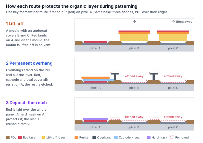
In lift-off, the organics sit on the mold and leave with it. In the Orthogonal 2014, Samsung Display 2016 and LG Display patents, the photoresist never touches the organics directly. A fluorinated layer goes down first, even over colors already made, and the pattern stands on it. Samsung Display 2018 covers them with a protective film and puts the photosensitive layer on top of that (Section 3.3). In the overhang method, the cathode and encapsulation film cover the organics first, and photoresist and etching are used on top of them. In deposit-and-etch, a hard mask goes on the organics and the rest of the organics is etched directly.
Of these, the two lift-off variants and the overhang method (AMAT) were turned into a 3D model of the whole process of drawing red, green and blue in turn. The organic layer, top electrode and encapsulation are deposited separately, so they are separate steps too.
3. Lift-off: peel it away with the mold
3.1 Cornell and Orthogonal, a solvent that does not dissolve
The root of the fluorinated photoresist is US8871545B2, filed jointly by Cornell University and the US startup Orthogonal. With a priority date of April 27, 2010, it claimed a “method of forming a multi-color OLED device.” It uses a fluorinated photoresist dissolved in a fluorinated solvent, which, unlike ordinary solvents, does not dissolve the organic layers, so the photoresist can go straight onto colors already made. There are two embodiments. One deposits the emitting layer over the photoresist pattern and peels it away with the photoresist (lift-off). The other lays the emitting layer first and etches it with O2 plasma using the photoresist pattern as a mask. Lift-off and the deposit-and-etch of Section 5 sit in the same patent. Its holders are still Cornell and Orthogonal.
Drawing pixels color by color with lift-off is older still. Princeton University’s US6013538A (priority November 24, 1997) describes depositing the organics through a photoresist patterning system with an undercut, covering them with a protective cap through the same system and then removing the photoresist, and the specification calls this step “lift-off.” The protective cap keeps the organic layer from the solvent during lift-off. The same specification says repeating the process can form devices of different colors side by side. What Cornell and Orthogonal’s 2010 patent added was writing down both lift-off and etching with a fluorinated photoresist that does not dissolve the organic layers.
Orthogonal refined this into a multicolor display process in a US provisional application of August 1, 2014. The published 2010 application is among the documents this family cites. The family patent US10468637B2 builds an undercut lift-off structure and removes the sacrificial layer with a fluorinated solvent that leaves the organic layers untouched. The part where the density is designed so the sacrificial layer curls up and floats away was covered in the DESK article. The current holder of this patent is Samsung Display.
FIG. 3 of the specification draws the whole process of making three colors in eleven scenes.
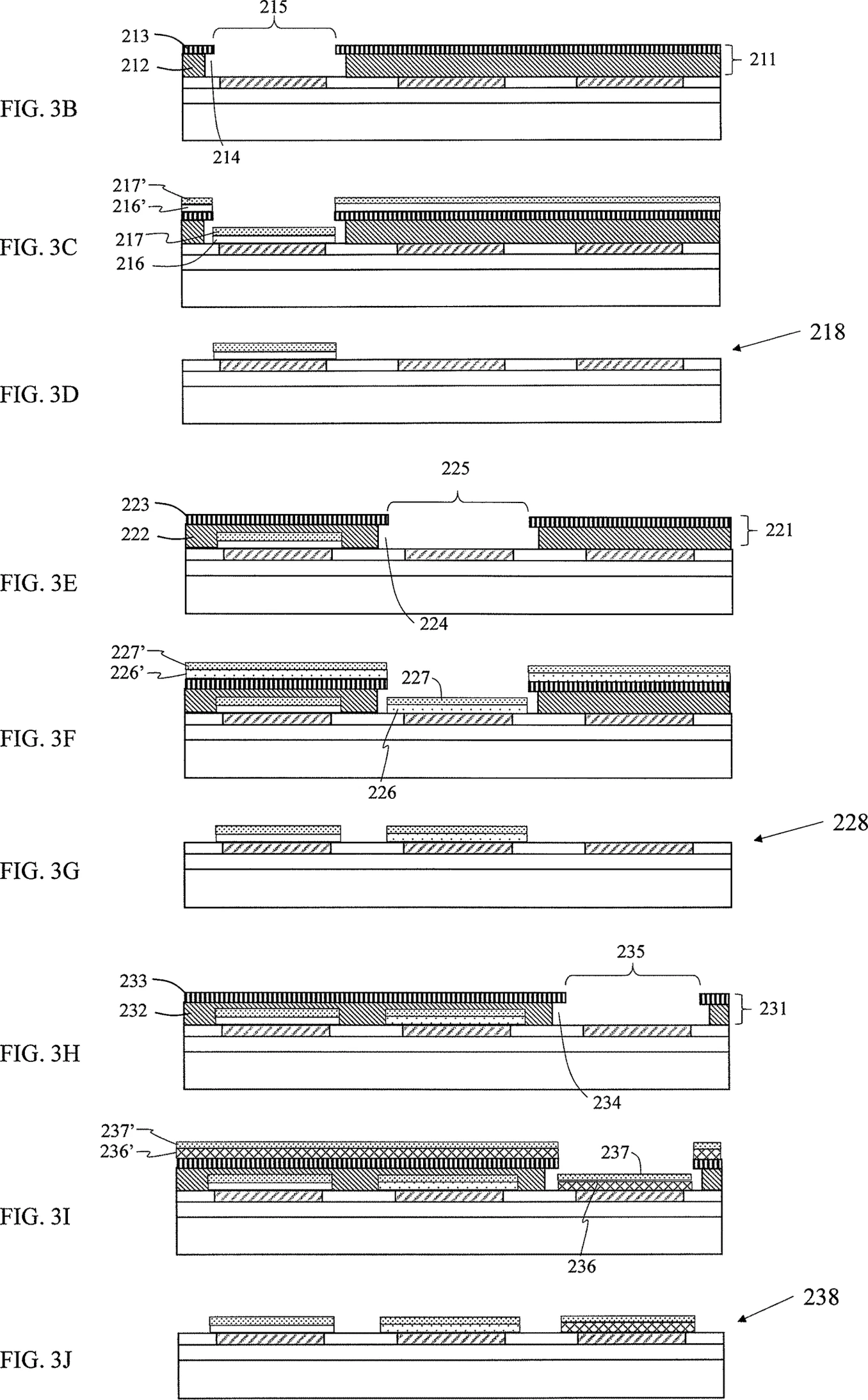
The new lift-off structures (221, 231) cover the pixels already made and open only the next site. Each earlier color hides under the mold every time and reappears when the mold is removed.
3.2 Samsung Display 2016, under its own name
Eight years before buying Orthogonal’s patents, in 2016, Samsung Display filed the same route with a fluorinated lift-off layer. Earlier Samsung Display filings are in Section 6.3. It is US10243175B2, with a Korean priority date of February 2, 2016.
A lift-off layer containing a fluoropolymer is formed on a substrate including a first electrode; on it is formed a pattern layer consisting of a first pattern layer of a material with higher surface energy than the lift-off layer and a second pattern layer of a material with lower surface energy than the first pattern layer; the lift-off layer between the patterns of the pattern layer is etched with a first solvent to expose the first electrode; an organic functional layer including an emitting layer is formed on the first electrode and the pattern layer; the remaining lift-off layer is removed with a second solvent; and a second electrode is formed.
US10243175B2 claim 1 summary (Samsung Display, priority 2016-02-02)The drawings show three colors in turn (FIGS. 4 to 6), and Figure 3 shows two of them. The specification describes as the basic case putting the cathode on as a common layer after all three colors are made, and also describes a variant in which an auxiliary cathode (181) is deposited on each color’s organic layer before lift-off.
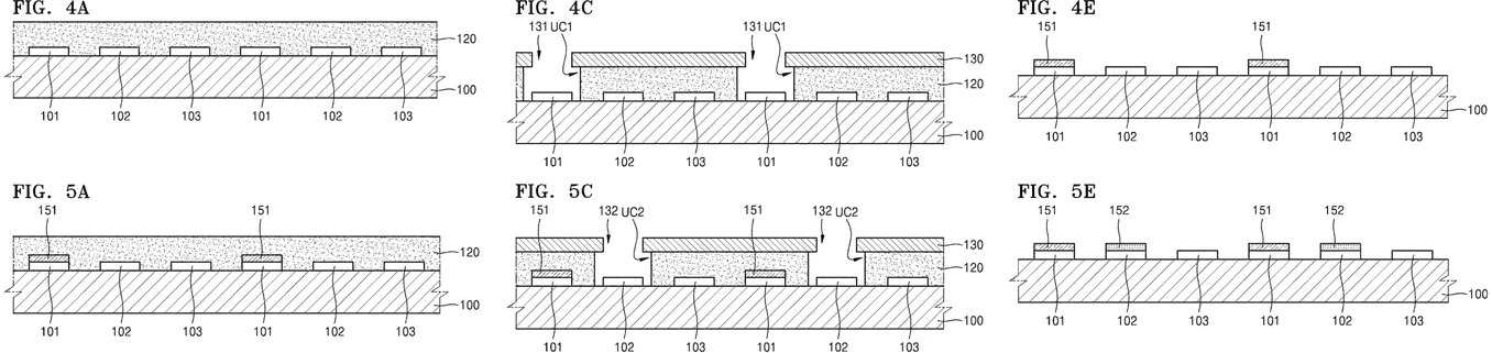
After the first color (151) is made, laying the lift-off layer (120) again covers the first color beneath it. Undercuts (UC2) are opened only at the second color’s sites, deposited on, and removed. Each earlier color hides under a new lift-off layer every time.
3.3 Samsung Display 2018, covering a protective film before removal
In 2018 Samsung Display added one step to lift-off. It is US11925071B2, with a Korean priority date of November 19, 2018. The background points to the method of “forming the emitting layer with a photoresist pattern and then removing the photoresist pattern by lift-off,” and notes that because lift-off is carried out exposed to the atmosphere, a protective film is needed to shield the emitting layer from atmospheric oxygen and moisture.
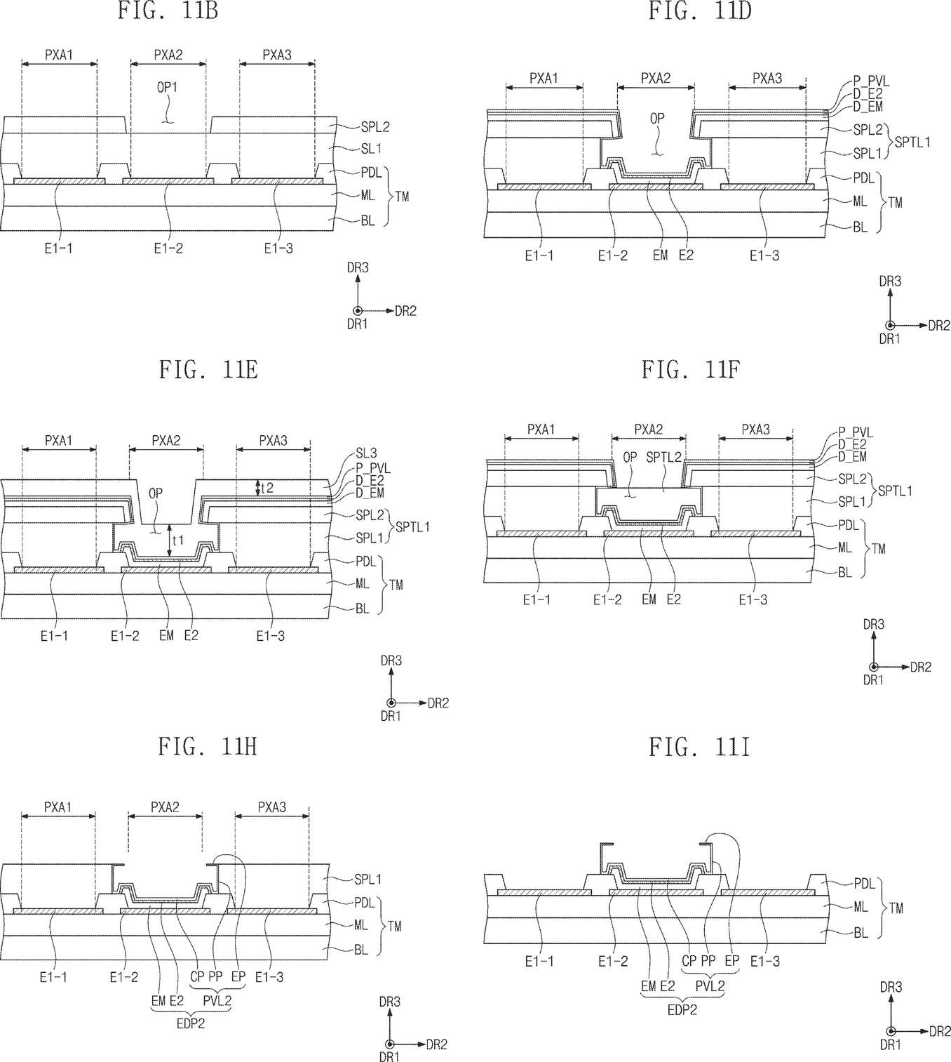
The order in the specification is this. A pattern layer is put on a first layer containing fluororesin to form an undercut, the emitting layer and electrode are deposited inside it, and a protective film covers them. A photosensitive layer is then put on to cover the inside of the opening, and the dummy layers piled on the pattern layer are etched first. Finally the pattern layer is removed. Wrapping the organic layers in a protective film before removal is what differs from the 2016 filing. Granted claim 1 also ties up a structure in which the electrode covering the emitting layer and the protective layer on it are separated pixel by pixel like islands.
3.4 LG Display 2021, the same principle
LG Display’s December 28, 2021 filing KR20230099873A (Korea, US, Europe, Japan, China, Taiwan) is the same route. Claim 1 ties up the shape of the sub-pixel pattern on the bank (an edge that thins toward the neighbor, and a trench over the bank hole), and the specification describes how to make it like this.
By using an undercut structure made of a double layer of a protective layer pattern of fluoropolymer material and a photoresist pattern, together with a lift-off method, multiple sub-pixel patterns can be formed easily even on large-area panels.
KR20230099873A specification, translated from the Korean original (LG Display, filed 2021-12-28)Of the protective layer, it says that thanks to an “orthogonal property” of having affinity for neither water nor oil, it is less affected by developers containing organic solvents. The background cites the difficulty of using FMM on large areas because of sagging.
The process is drawn step by step in drawings 4 to 19. First the bottom electrodes (122) are laid, and the bank (124) covering their edges is built (drawing 4). For each color, a fluorinated protective layer and a photoresist are laid, the photoresist is opened at that color’s sites, and the protective layer is etched further with a fluorinated solvent to form an undercut (drawings 5 to 7). When the organic emitting layer is deposited, the pixel pattern that goes under the undercut spreads onto the top of the bank and grows thinner toward its edge (drawings 9, 10). Full-surface lift-off with a fluorinated solvent then leaves only that color’s organic layer (drawing 11). The specification says the organic materials withstand fluorinated solvents, so the colors made earlier are not damaged. The second color (drawings 12 to 16) and the third (drawings 17, 18) follow the same order. The cathode (190) is formed over the whole surface after all three colors are made, and the encapsulation layer (197) goes on top of it (drawing 19). Orthogonal in Section 3.1, in its main embodiment, builds each color up to the top electrode before removal. The two orders can be seen side by side in the simulation in Section 2.
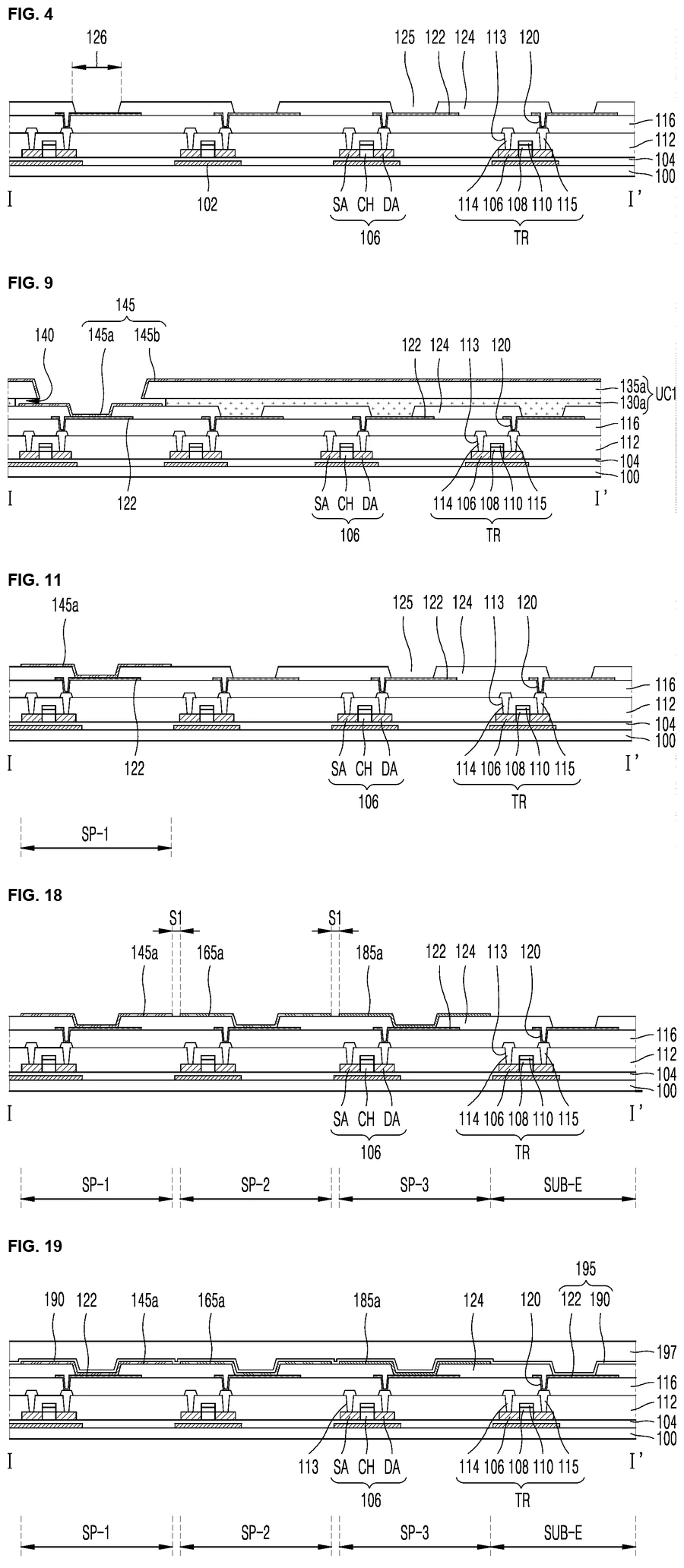
There is no evidence that this filing is FLiPP’s actual process. What this piece says goes only as far as this: LG Display filed on the lift-off route in 2021.
3.5 Samsung Display’s purchase of Orthogonal patents
On June 10, 2024, Samsung Display bought 5 US patents from Orthogonal. According to The Elec, 4 were “photolithographic patterning of organic electronic devices” and 1 was “color OLED display with larger aperture ratio” (US10468637B2), and at the time of the report the holder of the Korean family patents had not changed. The current holder on the US10468637B2 record is also Samsung Display. A company that filed the same route under its own name in 2016 bought Orthogonal’s 2014 family patents as well 8 years later. The 2010 Cornell and Orthogonal patent of Section 3.1 (US8871545B2) is not on this purchase list.
4. Etching (1), leaving an overhang: cut, seal, then etch
4.1 AMAT 2020, the particle problem of lift-off
Overhang partitions themselves are old. In US5701055A of 1994, Pioneer claimed an organic EL display panel with insulating ramparts between pixels that have an overhang projecting sideways. Within the range this piece found, the first to combine an overhang, per-pixel encapsulation and etching to draw pixels color by color without an FMM was the equipment maker Applied Materials (AMAT). In its background, US11476313B2 (published as US20220077257A1), with a priority date of September 4, 2020, rejected lift-off.
Rather than utilizing a fine metal mask, photo lithography should be used to pattern pixels. Currently, OLED pixel patterning requires lifting off organic material after the patterning process. When lifted off, the organic material leaves behind a particle issue that disrupts OLED performance.
US20220077257A1 background (AMAT, priority 2020-09-04)Instead, an inorganic overhang is built on the pixel-defining layer. Claim 1 of the publication (US20220077257A1) says the overhang sets the deposition angle so that the organics go in under the overhang and the cathode reaches past the edge of the organics to touch the overhang. The broken cathode is connected through a conductor on the overhang side (Section 6.3).
It also draws the order of switching colors.
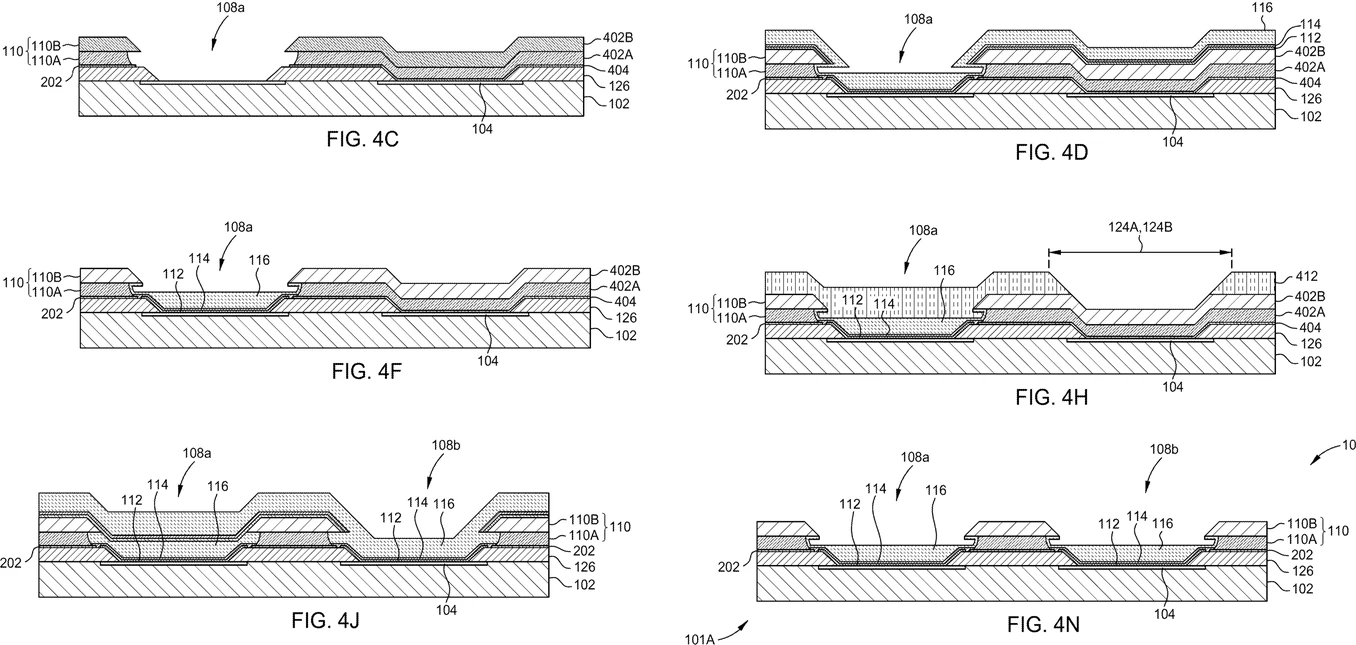
The key is that the overhangs are not all made at the start. The overhang material layers are laid over the whole surface and only the first sub-pixel site is opened. The first color, cathode and encapsulation are deposited, resist is placed in the first pixel well, and the rest is wet-etched. For the second color, the resist covers the first sub-pixel while only the second site is opened and the same process is followed. Sites not yet opened are covered by the overhang material layers, and finished pixels by the resist (in the plug arrangement, a protective film 414 is added). The specification says “the same steps are repeated for each additional sub-pixel.”
In WO2022225657A1, with a priority date of April 23, 2021, AMAT separately claimed the overhang structure itself. Claim 1 stacks the overhang from three metal layers of different compositions (base, body and top), and the conductive oxide in the title appears in dependent claims as a base-layer material. The same background sentence appears again.
This route did not stop at patents. On November 21, 2024, AMAT announced “MAX OLED” and said it simplifies scaling from Gen 6 to Gen 8 substrates. It said an alpha system would be supplied to Samsung Display for evaluation. AMAT’s invited paper at SID 2025 describes MAX OLED as a package of an overhang structure, angle-controlled deposition and thin-film encapsulation over each pixel. Its author list includes six inventors of the two patents above.
What happened next has not been disclosed by the company and is known only from press reports. The Elec reported on October 19, 2026 that in September 2025 Samsung Display brought a Gen 5.5 quarter-size vertical evaporator from AKT, an Applied Materials affiliate, into its Asan A2 line to evaluate non-FMM technology, but that it did not fit the existing small-to-medium and medium-to-large development roadmaps. The article did not call the tool MAX OLED. According to the same article, development of Samsung Display’s in-house MPO (Micro Patterned OLED) technology was effectively on hold until early 2026 and a project has been under way since March 2026, aiming at a 7-inch engineering sample. On the same day, Electronic Times reported that Samsung Display has begun talks with suppliers on an inkjet OLED pilot line and, quoting an industry source, that it has picked inkjet among non-FMM technologies.
4.2 JDI 2022, titanium and oxide overhangs
JDI announced eLEAP in May 2022. Three and a half months before that, US12520704B2, with a Japanese priority date of January 27, 2022, claimed an overhang structure.
The partition includes a lower portion placed on the rib and an upper portion placed on the lower portion with an end protruding beyond the side surface of the lower portion, the upper portion including a first layer made of titanium and a second layer made of a conductive oxide… the upper electrode is in contact with the partition.
US12520704B2 claim 1 summary (JDI, Japanese priority 2022-01-27)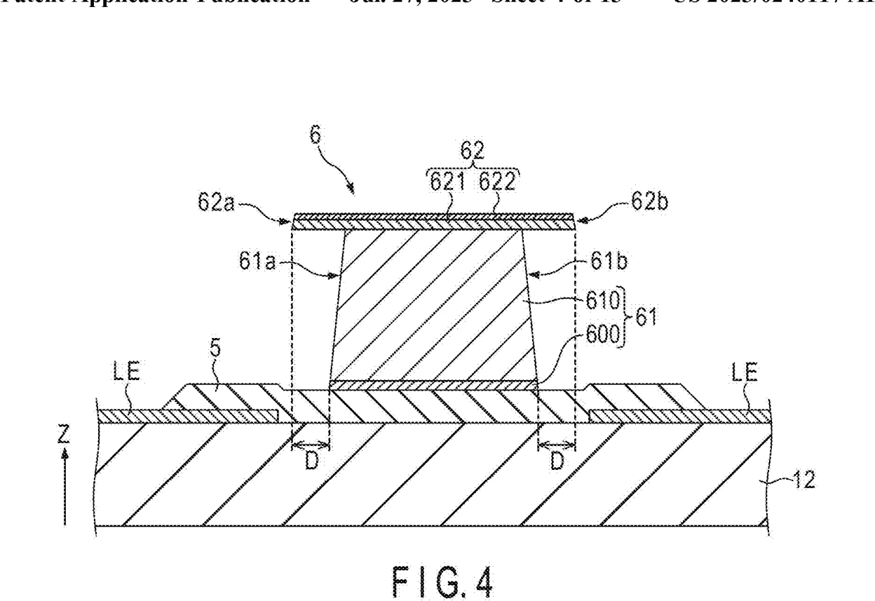
Depositing, covering everything up to encapsulation, and etching on top is the same as AMAT. But JDI builds all the partitions first (FIGS. 6 to 10). The organic layer, upper electrode, cap layer and encapsulation layer are then deposited over the whole surface, and the overhang cuts the organic layer and the electrode. Resist is placed on the encapsulation layer and the exposed parts are dry-etched. JDI’s drawings, however, go only as far as the first color, and for the other colors it says only that “similar processes are performed in turn.” The JDI patent cites AMAT’s 2021 overhang document.
There is also a filing that claims the etching steps themselves: US12501819B2 (published as US20230225180A1), with a Japanese priority date of January 13, 2022, half a month earlier.
First and second organic layers and first and second upper electrodes are formed over the overhanging partition, an encapsulation layer is formed on them, a resist covering part of the encapsulation layer is formed, anisotropic dry etching is performed using the resist as a mask to thin the exposed encapsulation layer, and isotropic dry etching then removes the exposed encapsulation layer.
US20230225180A1 (granted as US12501819B2) claim 1 summary (JDI → Magnolia White, Japanese priority 2022-01-13)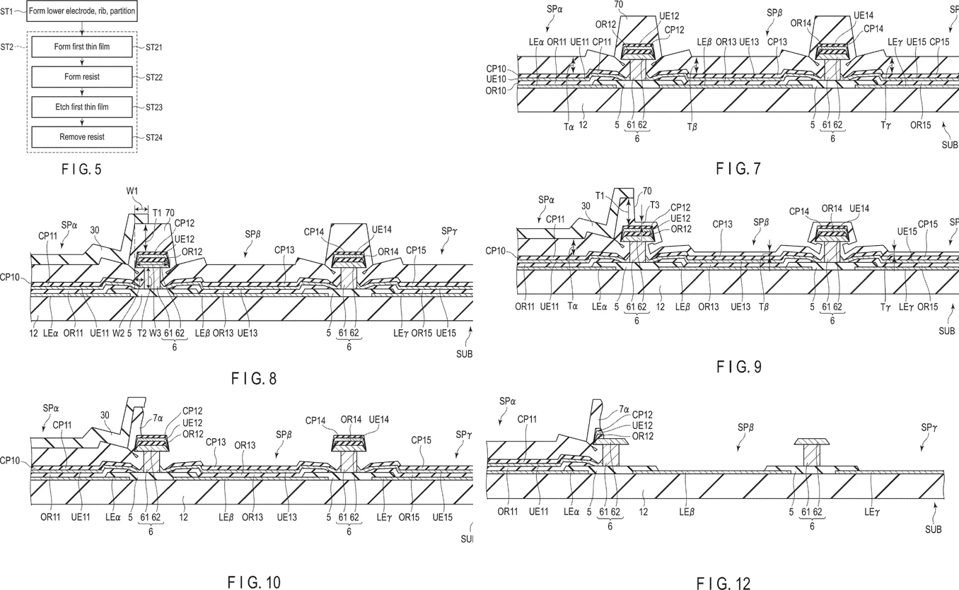
This patent, too, was assigned to Magnolia White on June 27, 2025.
4.3 Visionox 2022, T-shaped isolation parts that stay
Visionox announced ViP in May 2023. Nine months before that, CN117500332A (with international, Korean and US filings), with a priority date of August 2, 2022, set out the structure and order of the overhang route.
The support layer includes a first sub-part and a second sub-part located closer to the substrate, and the orthographic projection area of the first sub-part on the substrate is larger than that of the second sub-part. The support layer encloses an isolation space, and the sidewall of the support layer is recessed toward the isolation space to form a groove. The emitting layer includes an emitting unit inside the isolation space, and at least part of the first encapsulation portion of the encapsulation layer lies inside the groove.
CN117500332A claim 1 summary, translated from the Chinese original (Visionox, priority 2022-08-02)The support layer, wide at the top and narrow at the bottom, is the overhang. The drawings show three colors in turn.
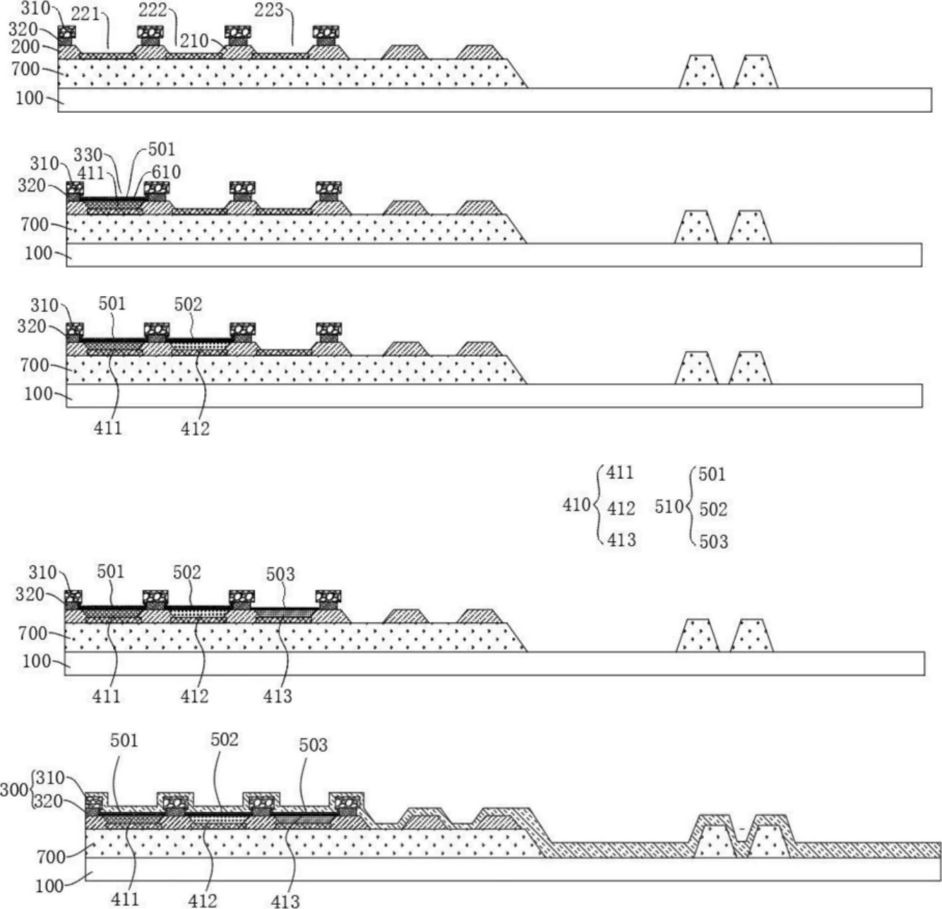
The specification says that for each color, an emitting material layer, an electrode material layer and an encapsulation sub-layer are laid and patterned to make that color’s emitting unit and encapsulation sub-part. Each color gets its own encapsulation, and at the end a second encapsulation portion covers everything.
WO2024198939A1, with a Chinese priority date of March 31, 2023, is a variant. The emitting layer and electrode are deposited inside a metal isolation structure and sealed, and then the isolation structure is etched away. The specification says “there is no need to use a precision mask to evaporate the light-emitting layer,” which simplifies the process and can raise resolution.
5. Etching (2), no overhang: lay it everywhere and etch with a hard mask
The root of deposit-and-etch is also the 2010 Cornell and Orthogonal patent of Section 3.1. Its second embodiment lays the emitting layer everywhere and etches it with O2 plasma using a fluorinated photoresist pattern as the mask. Japan’s Semiconductor Energy Laboratory (SEL) wrote down a way to put an inorganic hard mask, instead of photoresist, on the organics. It is WO2022123382A1, with a Japanese priority date of December 7, 2020. The specification calls a structure that uses neither a metal mask nor an FMM an “MML (metal maskless) structure.” This embodiment, however, forms the counter electrode with a metal mask (190), so by the specification’s own definition it is an MM structure.
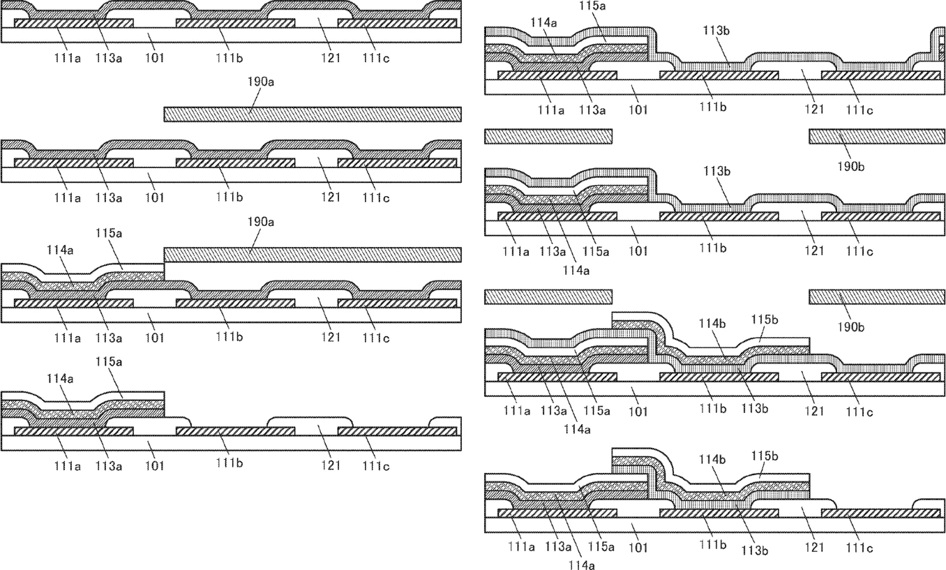
A first layer (EL layer) is formed; a first metal mask having a first opening is placed over it and a film is formed to make a first counter electrode overlapping a first pixel electrode; and, using the first counter electrode as a hard mask, the region of the first layer overlapping a second pixel electrode is removed. A second layer is then formed… and removed using a second counter electrode as a hard mask.
WO2022123382A1 claim 1 summary (SEL, Japanese priority 2020-12-07)The organic layer is laid over the whole surface, and the counter electrode is put only on the pixels to be kept, serving as the hard mask. When the second color is laid over the whole surface it also piles up on the first pixel, but the first pixel’s counter electrode protects what is beneath. Neither a mold nor an overhang is needed. Another SEL document (US12300126B2) also describes covering the EL film with a sacrificial film and etching the organic layer with resist.
The same month, SEL claimed a method of etching colors in turn with sacrificial films. It is WO2022144666A1, with a priority date of December 29, 2020. Claim 1 covers two colors, and the drawings show three.
A first EL film is formed on first and second pixel electrodes, a first sacrificial film covering it is formed, the first sacrificial film and first EL film are etched to expose the second pixel electrode… a second EL film and second sacrificial film are formed and etched, and after the first and second sacrificial layers are removed the EL layers are dried. The EL films are removed by dry etching, and the sacrificial layers by wet etching.
WO2022144666A1 claim 1 summary (SEL, priority 2020-12-29)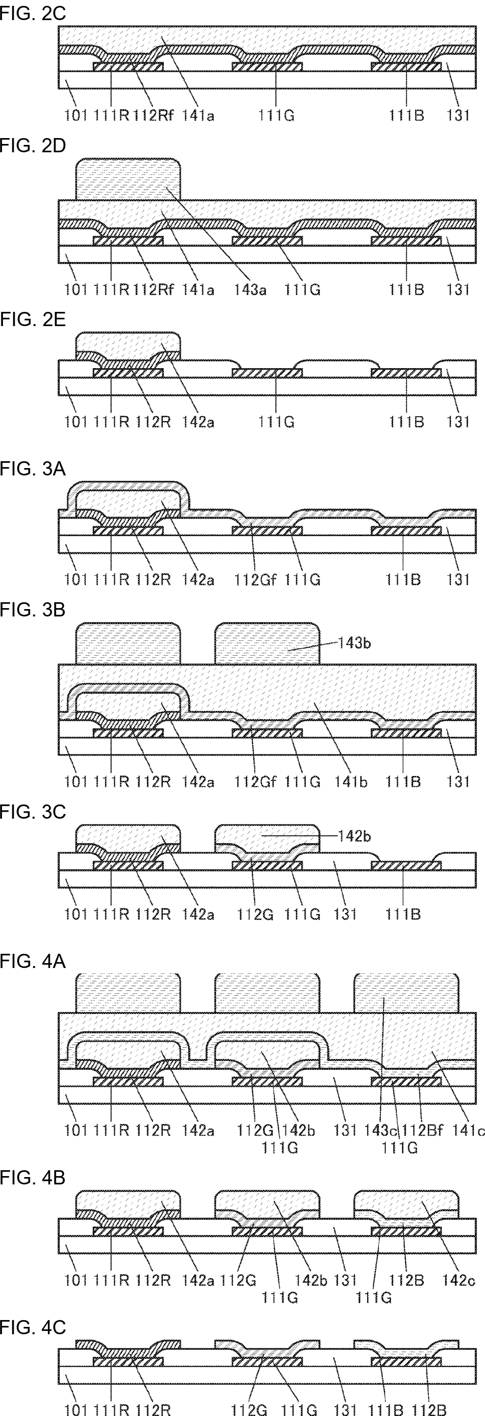
While the next color is being etched, the colors made earlier sit under their own sacrificial layers (142a, 142b). After all three colors are done, the sacrificial layers are all removed by wet etching.
6. Why the overhang stays, and what it connects
6.1 The PDL cannot cut the films
Without an FMM, the organics are laid over the whole panel. To handle each color separately, the films have to be cut between pixels. The PDL cannot do this: its sides slope gently, so films laid over it pass across without breaking. So one more eave is built on top of the PDL. AMAT’s publication (US20220077257A1) says the overhang casts a shadow during evaporation and so sets the deposition angles of the organics and the cathode.
An eave that cuts films is not a new idea. Pioneer’s 1994 filing (US5701055A) claimed an organic EL display panel with insulating ramparts between pixels that have an overhang projecting sideways. Those ramparts are insulators, and their job ends at cutting. The eave in the overhang method cuts and then connects again.
6.2 If the eave stays, the top electrode goes on color by color
If the eave stays in the panel, a common cathode laid after all three colors is cut again at the eave. The three companies’ patents in Section 4 all lay a top electrode for each color. AMAT deposits OLED material, cathode and encapsulation for each color and then wet-etches the rest. JDI lays the organic layer, top electrode, cap layer and sealing layer and keeps only what is under the resist. Visionox lays a light-emitting material layer, an electrode material layer and an encapsulation sub-layer for each color and patterns them. Among the overhang patents this piece read, none lays the top electrode after all three colors.
The side where the eave does not stay is different. LG Display’s 2021 lift-off lays the cathode (190) once after all three colors (Section 3.4). Even with etching, SEL’s sacrificial-film method (WO2022144666A1) lays a common electrode after all the sacrificial layers are removed. What makes laying the top electrode color by color unavoidable is not etching but the eave that stays. In lift-off, laying it color by color is a choice.
6.3 What connects the separated top electrodes
Top electrodes laid color by color end up as islands, one per pixel. The three companies’ patents describe connecting them through a conductor on the eave side (an optional embodiment for Visionox). Claim 1 of AMAT’s publication says the cathode goes in under the eave, past the edge of the organics, and touches the eave. Of the four eave configurations in the same specification, two have a conductive lower portion, and the other two have a non-conductive lower portion with an assistant cathode beneath it. AMAT’s 2021 filing (WO2022225657A1) puts it this way.
The conductive base portion 110A ensures permanent connection to the cathode 114.
WO2022225657A1 specification (AMAT, 2021-04-23 priority)JDI’s claim 1 says the upper electrode is in contact with the partition, and its specification says the lower portion (61) of the partition is conductive and is connected to a power supply outside the display area, applying a common voltage to the upper electrode of each pixel. Visionox’s specification says the electrodes of adjacent light-emitting units can be connected to each other through the isolation part, and leaves making that part of metal as an optional embodiment.
Connecting top electrodes that are separated pixel by pixel can also be done with lift-off, which leaves no eave, and it appears in Samsung Display filings earlier than AMAT’s. US10038037B2 (Korean priority September 3, 2015) connected counter electrodes separated pixel by pixel through a connection electrode layer on the pixel-defining layer. US10403853B2 (Korean priority June 16, 2016) covered island-shaped counter electrodes with wider island-shaped protective layers and connected the counter electrodes through a connection layer above them; it performs lift-off for each pixel using a photoresist mold. US10727433B2 (Korean priority April 30, 2018) connected neighboring counter electrodes through an auxiliary electrode on an inorganic pixel-defining layer and tied that auxiliary electrode to a power supply line outside the display area. Within the range this piece found, Samsung Display’s filings wrote down laying an electrode and protective film for each color and connecting the separated electrodes before AMAT did. Samsung Display’s filings cut the films with a photoresist mold and removed it by lift-off; AMAT 2020 cut them with an inorganic overhang that stays in the panel and removed the rest by etching.
Encapsulation wraps the ends. AMAT’s publication says the local encapsulation (116) laid over each pixel goes in under the eave and runs up its sidewall. The 2021 filing describes covering under the eave as the basic case and, in some embodiments, covering the top surface as well. Because the edges of the organics and cathode end under the eave, the encapsulation wraps those ends. A global passivation layer (120) then covers the eaves and the local encapsulation.
6.4 Films laid again for each color
Which films are laid again for each color differs by route. In LG Display’s 2021 lift-off, the organic light-emitting layer laid for each color includes the hole and electron transport layers, and the specification says the undercut depth cuts the charge generation layer of the tandem structure to prevent leakage. Laying common layers again for each color happens in lift-off too. In all three companies’ overhang patents read, the cathode and local encapsulation also go on for each color. In lift-off this is optional (per color in Orthogonal’s main embodiment and Samsung Display 2018, after all three colors in LG Display 2021). With three colors, the overhang method lays the cathode and local encapsulation three times, and each time the films over the other colors’ sites are etched away. How much more material this uses is not in the patents, and this piece did not check it.
7. Comparative analysis
7.1 The three routes side by side
| Lift-off | Etching, overhang stays | Etching, no overhang | |
|---|---|---|---|
| How unwanted organics are removed | Lift-off (peeled away with the mold) | Etching | Etching |
| Does resist go on the organics? | Mostly not in direct contact (it stands on a fluorinated layer). Samsung Display 2018 puts it on the protective film | It goes on the cathode and encapsulation film | A hard mask (counter electrode, sacrificial film) covers them |
| Structure left in the panel | None | Overhang (partition) | None |
| What protects earlier colors | A new lift-off layer | Resist while the next site is opened (AMAT, plus protective film 414 in the plug arrangement), then that color’s encapsulation (AMAT, JDI, Visionox) | That pixel’s counter electrode or sacrificial layer |
| When the top electrode goes on | Per color (Orthogonal main embodiment, Samsung Display 2018), after all three colors (Samsung Display 2016, LG Display, Orthogonal FIG. 7 embodiment) | Per color, including cathode and encapsulation. The separated cathodes are connected through a conductor on the eave side (Section 6) | Per color (SEL 2020, counter electrode as hard mask), after all three colors (sacrificial film method) |
| First to write down the principle (within the range found) | Princeton 1997 (photoresist undercut lift-off), Cornell and Orthogonal 2010 (fluorinated photoresist) | AMAT 2020 (overhang, per-pixel seal and etching combined) | Cornell and Orthogonal 2010 (photoresist mask), SEL 2020 (inorganic hard mask) |
| Panel maker filings | Samsung Display 2016 and 2018 (earlier 2015 to 2018 filings in Section 6.3), LG Display 2021 | JDI 2022, Visionox 2022 | |
| Weaknesses stated in the texts | AMAT: lift-off leaves a particle problem |
7.2 Who, and when
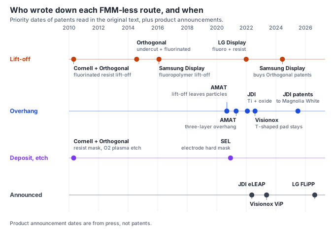
The principles were first written down outside the panel makers between 1997 and 2020. The panel makers’ filings followed, and product announcements came after those. Among filings that divide colors without an FMM, the earliest panel maker is Samsung Display. It filed lift-off applications under its own name from 2015, five years before the AMAT and SEL filings (Section 6.3).
7.3 Who followed the Orthogonal patent?
Documents citing Orthogonal’s US10468637B2 were counted by applicant.
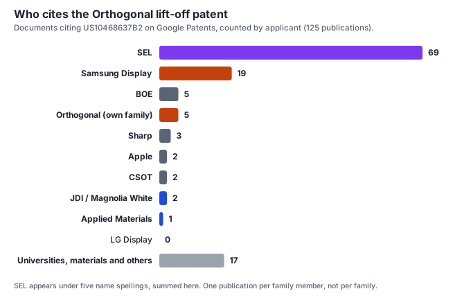
More than half, 69, are SEL’s. All but one were filed after December 2020. Samsung Display follows with 19, the earliest being its own 2016 filing from Section 3.2. LG Display has 0. The 19 documents cited in the LG filing from Section 3.4 were all added by the examiner, and no Orthogonal document is among them.
8. Where the overhang patents went
The current holder of JDI’s two patents from Section 4.2 (US12520704B2, US12501819B2) is not JDI. Both records state that they were assigned to “MAGNOLIA WHITE CORPORATION” on June 27, 2025.
JDI’s timely disclosure of June 26, 2025 explained how. On May 19, 2025, JDI and its subsidiary JDI Design and Development set up three dedicated intellectual property subsidiaries (Magnolia Purple, White and Blue) and transferred part of their LCD and OLED display patents to them as contributions in kind. They then decided to transfer all shares of the three companies to the side of their largest shareholder, Ichigo Trust. According to the disclosure, Ichigo Trust is the controlling shareholder with 78.20% of JDI’s voting rights, JDI had borrowed 65 billion yen from this fund. A basic agreement of May 15 provided for transferring these shares together with the land and buildings of the Mobara plant and repaying the 65 billion yen with the proceeds. The disclosure, however, says the share transfer would go first “to secure working capital for the time being,” and that talks on transferring the plant property were continuing. The July 30 disclosure says that, at Ichigo’s wish, the transferee was changed to Magnolia Unitas, a 100% subsidiary of a company 100% funded by Ichigo, and that the transfer was completed that day. The transfer price was not disclosed.
JDI received a royalty-free license to the transferred patents. The disclosure says JDI keeps some patents related to new businesses and to displays it continues to produce.
9. Counterevidence and limitations
There is no evidence that LG Display’s 2021 filing is FLiPP’s actual process. LG has described FLiPP as its own technology and has not disclosed process details. This piece states only that an LG filing on the same route exists. The company’s announcement said precise UV etching erases what is not needed, and The Elec (2026-10-19) reported that FLiPP deposits the organics widely and removes the unwanted parts with photo processing and etching, with the isolation structure that cuts the organics remaining in the final product. If that report holds, FLiPP is closer to the overhang side than to the lift-off of LG’s 2021 filing. That too is a press report, not a process the company has disclosed.
It is a fact that the LG Display filing does not cite Orthogonal documents. What that means cannot be told from the documents.
Whether Samsung Display mass-produces with lift-off was not checked. The patent filings and purchase are facts, but the actual process choice has not been disclosed. The MPO and inkjet efforts in Section 4.1 are press reports citing the industry, not company statements. The Elec says MPO first builds an isolation structure, forms the organics only where needed, does not etch the organic layer afterwards, and removes the structure during manufacturing. That description resembles both this piece’s lift-off and Visionox’s 2023 filing, which removes the isolation structure by etching. In 2015 to 2018, Samsung Display filed several applications that lay a counter electrode for each color and connect the separated electrodes (Section 6.3). Press reports alone cannot settle which MPO is.
The three routes divided by the two questions are this piece’s division (Section 2). Real processes can mix them. There are also methods, like Visionox’s 2023 filing, that cut with a structure and then remove it.
Section 6.2’s reading that the eave stays and cuts even a common cathode, so the top electrode goes on color by color, is an interpretation drawn from the process order of the three companies’ overhang patents. The patents do not state that reason.
The process drawings included are mainly those showing the order of switching colors. The JDI patents draw only the first color, and do not say how the earlier pixels are protected for the later colors. Figure 1 draws only one scene of the first color for all three routes.
Each company’s earliest filing, and who wrote a principle down first, are within the range this piece confirmed. Photoresist undercut lift-off (Princeton 1997) and overhang ramparts (Pioneer 1994) already appear in 1990s documents.
10. Conclusion and implications
The technology for doing away with the FMM reads as two questions: whether the organics are peeled away with a mold or etched, and whether an eave cutting the pixels apart is left. The overhang is not a third method but a structure paired with etching. If the eave stays, a common cathode is cut too, so the overhang method lays the cathode and encapsulation for each color and describes connecting the separated cathodes through a conductor on the eave side (an optional embodiment for Visionox). Lift-off, where the eave is removed, and sacrificial-film etching, which has no eave, can lay the top electrode after all three colors.
The principles were first written down outside the panel makers. Lift-off was first written down by Princeton University in 1997, etching with a photoresist mask by Cornell University and the startup Orthogonal in 2010, and the overhang method by the equipment maker AMAT in 2020; the one that refined etching without an overhang with an inorganic hard mask was the research lab SEL. The panel makers’ filings came after them. By their filings, Korea’s two companies sit on the lift-off side, and JDI and Visionox on the overhang side. Samsung Display, however, decided to bring in an alpha system of AMAT’s overhang-based MAX OLED, and in October 2026 reports said it is pursuing an in-house MPO prototype and an inkjet pilot line. The actual process choice is not yet settled.
Mass production has not yet said which will win. On the patent side, though, some things have already been settled. On lift-off, Samsung Display bought and holds Orthogonal’s 2014 family patents, while JDI, on the overhang side, handed part of its own patents to its controlling shareholder’s side to secure working capital and received a royalty-free license.
Two things are worth watching. One is how the process of LG Display’s FLiPP shows up in patents. LG’s 2021 filing is on the lift-off side, but the company’s announcement spoke of etching and press reports say the isolation structure stays (Section 9). If it is on the overhang side, where it overlaps with the claims of AMAT, JDI and Visionox becomes the next question. The other is SEL. The one that cited the Orthogonal patent most was not a panel maker but a research lab. Which panel maker’s process those filings lead to is the second question.