Tandem OLED Charge Generation Layer (CGL): A 430-Patent Analysis
The charge generation layer (CGL) that links emission units in a tandem OLED traces its architecture to a 2002 Kodak patent, which expired in 2022. Korea's two panel makers spent 2013-16 refining the CGL material itself, then shifted after 2017 toward pixel-level structure — and on the shared problem of current leaking sideways into neighboring subpixels, Samsung cuts the CGL apart while LG pins its potential in place instead. China, starting 10 years later, is now claiming both stages of that progression at once.
1. Overview
1.1 Stack two layers, and you get a seam
A tandem OLED stacks two or more emission units vertically and drives them all at once with a single pair of electrodes. To produce the same brightness, the current each unit receives is reduced, which extends lifetime. The panels Samsung Display and LG Display supply for Apple’s OLED iPad are two-stack (two-tier) tandem structures.
In February 2026, Samsung Display increased the number of blue emission stacks in QD-OLED from four to five and released the structure under the name “Penta Tandem.” According to the company’s own announcement, luminous efficiency rose 1.3x and lifetime doubled. The number of stacks keeps climbing.
To stack layers, you need a thin film that electrically links one layer to the next. It’s the film that feeds electrons into the unit below and holes into the unit above, so the two units light up in series. This film is called the charge generation layer (CGL). This piece reads the patents behind that seam.
1.2 Scope of analysis
| Item | Value |
|---|---|
| Population | Documents on Google Patents whose claims contain “charge generation layer”: 1,392 documents — US filings from LG Display and Samsung Display, and US/Chinese filings from five Chinese companies (BOE, CSOT, Visionox, Tianma, EverDisplay) |
| Tandem claims | Of those, 494 documents whose independent claims contain a CGL, grouped into families (by applicant + priority date + invention title) into 430 families |
| Classification | Read the characterizing portion of claim 1 of each and classified it by “what it additionally limits.” Eight documents that used CGL to mean something else, such as a hole injection layer, were excluded → 422 families (LG Display 157 · Samsung Display 95 · five Chinese companies 170) |
| Classification check | 48 documents chosen at random were reclassified from the full claim text: exact match on 39 (81%), match at the level of “is it the CGL itself or not” on 41 (85%) |
| Root tracing | All prior patents cited by the 208 tandem-patent families of the two companies. Early patents were confirmed against the original text |
| China’s starting point | Of Chinese Patent Office documents with CGL in the claims and a priority date before 2015, 744 were narrowed to mainland Chinese applicants and confirmed against the original text |
1.3 Terminology
2. Who first claimed the tandem seam?
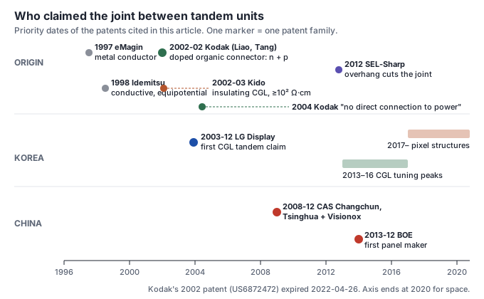
The series-stacked structure itself was first claimed by US-based eMagin in 1997, and the “organic connecting layer doped n-type and p-type” that forms the backbone of today’s LG Display and Samsung Display claims was claimed by Kodak in February 2002. That Kodak patent expired on April 26, 2022.
2.1 From metal conductor to doped organic layer
In a patent provisionally filed in July 1997 (US6337492B1), eMagin stacked OLEDs vertically with a metal/ITO conductive layer in between. The specification states that the current to each stacked device is not controlled separately. A single current flows through the whole stack in series.
Japan’s Idemitsu Kosan, in a 1998 filing (JPH11329748A), connected multiple emission layers in series through an intermediate conductive layer. Up to this point, the seam between units was a good electrical conductor.
Kodak’s Liang-Sheng Liao and Ching W. Tang, in a patent with a February 2002 priority date (US6872472B2), replaced this intermediate layer with an organic material instead of a metal. Claim 1 runs four lines.
A stacked organic electroluminescent device comprising: (a) an anode, (b) a cathode, (c) a plurality of organic electroluminescent units disposed between the anode and the cathode, and (d) a doped organic connector layer disposed between each pair of adjacent organic electroluminescent units.
US6872472B2 claim 1 (Kodak, priority 2002-02-15)The reason the specification gives is light. It states that in earlier stacked structures that place an electrode between units, that electrode absorbs light, lowering overall light output, and that making it thin raises its resistance. What was placed there instead is a connecting layer made of an n-type doped layer and a p-type doped layer.
The specification even sets out the materials. The n-type dopant is a metal with a work function below 4.0 eV, particularly an alkali metal or its compound. The p-type dopant is a strong electron acceptor that forms a charge-transfer complex by taking electrons from the host, and the p-type host is an aromatic tertiary amine such as NPB. Doping concentration is 0.01-10 vol%, and the connecting layer thickness is roughly 1-100 nm.
2.2 Why did Kido claim an insulating CGL?
A month later, in March 2002, a team around Professor Junji Kido of Yamagata University put a charge generation layer name on the same-position layer and set the opposite condition. Claim 1 of the earliest US filing (US20030189401A1) limits this layer to being an electrically insulating layer with a resistivity of 1.0×10² Ω·cm or greater.
The reason is written in the specification. As with the Idemitsu filing, if a highly conductive material is used to divide the units, “the light-emitting area becomes difficult to define as desired because of conductivity in the planar (lateral) direction.” The lateral-leakage problem that Korean and Chinese panel makers wrestle with today was already in a 2002 specification.
This original application was abandoned, and a divisional application (US8080934B2) was granted and expired on October 3, 2025. The granted claim limits the CGL to containing an electron acceptor and an electron donor, with a resistivity roughly equal to that of the adjacent organic layer.
In its 2004 white tandem patent (US7273663B2), Kodak nailed down the character of the seam in the claim itself. The intermediate connecting layer between units “is not directly connected to an external power source.” In other words, it is a floating layer. This one line returns in Section 4.
2.3 The prior art most often cited against the two companies’ patents
We counted the full citation lists of the 208 US tandem-patent families in which LG Display and Samsung Display placed a CGL in an independent claim. Among external prior patents with a priority date before 2006, Kodak (including current rights holder Global OLED Technology) was cited most often, 116 times. Semiconductor Energy Laboratory (SEL) followed with 30, Sony with 28, and Kido/Rohm with 22.
eMagin’s 1997 patent, which first claimed series stacking, was cited once; Idemitsu’s 1998 filing, zero times. The patent that claimed it first and the patent most often placed as prior art against the two companies’ patents were different. Kido’s 2002 filing was cited only on the Samsung side.
3. What have Korea’s two companies been claiming?
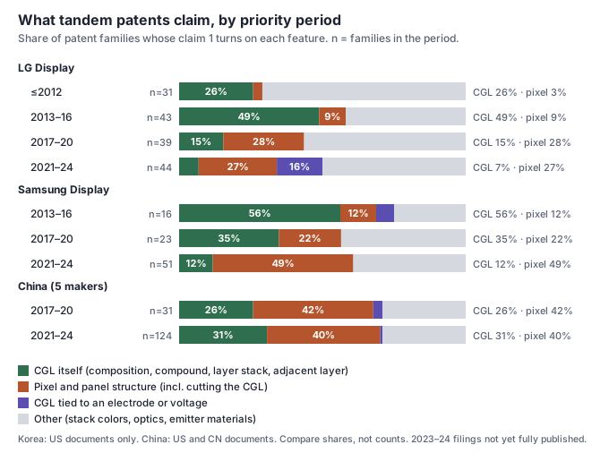
LG Display’s and Samsung Display’s tandem claims peaked at refining the CGL itself in 2013-16, then shifted after 2017 toward pixel- and panel-level structure. The share of families that limit the CGL itself fell from 49% (2013-16) to 7% (2021-24) at LG Display, and from 56% to 12% at Samsung Display.
3.1 2013-16: Refining within Kodak’s frame
Claims from this period do not re-claim the n-type/p-type connecting layer framework that Kodak set out in its specification. They twist one element within that framework.
| Patent | Priority date | What claim 1 additionally limited |
|---|---|---|
| LG Display US8912534B2 | 2012-04 | A p-type CGL made only of organic materials, with one of the organics having a LUMO of −6.0 to −4.5 eV |
| LG Display US9065068B2 | 2013-10 | An n-type CGL with two hosts of different LUMO plus a dopant |
| Samsung Display US20180026084A1 | 2016-07 | A CGL containing a perovskite-structured metal compound |
| LG Display US10014357B2 | 2016-09 | A p-type CGL of a single organic material, and an n-type CGL split into three zones with a stepwise dopant concentration |
| Samsung Display US20180114939A1 | 2016-10 | A dopant concentration gradient in at least one of the n-type and p-type CGLs |
Kodak’s specification named an alkali metal as the n-type dopant and a strong electron acceptor as the p-type dopant. All five of the above build on that range, varying the number of hosts, whether doping is present, and the distribution of concentration.
We also checked whether this claiming had moved to material suppliers. Of 76 Duksan Neolux documents with CGL in the claims, not one claimed the CGL material itself. All were dependent claims to the effect of “a device using that compound qualifies if it has two or more stacks including a CGL.” In 2013-24, the material suppliers that directly claimed CGL compounds were LT Materials (10 documents), LG Chem (5), and Novaled (2).
3.2 After 2017: Toward pixel structure
Families that limit the CGL itself fell not just in share but in raw count. LG Display had 21 in 2013-16, 6 in 2017-20, and 3 in 2021-24. Over the same periods, LG Display’s total tandem families were 43, 39, and 44 — they did not shrink.
What filled that space was pixel- and panel-level structure. Of Samsung Display’s 51 tandem families in 2021-24, 25 (49%) limited the structure between pixels in claim 1. Of those, 14 contain language about cutting the CGL or blocking leakage. What they are trying to block is covered in the next section.
Claims that limit the number of stacks and their color composition continue as well. Samsung Display’s 2022 filing (US20230320120A1) claims five or more emission units stacked, with the first and second units emitting green and the third through fifth emitting blue. It is still under examination, and whether it matches the structure of the company’s announced Penta Tandem product could not be confirmed from public materials.
4. How do Samsung and LG block current leaking into neighboring subpixels?
Facing the same lateral-leakage problem, Samsung Display mainly claims structures that physically cut the CGL at pixel boundaries, while LG Display, alongside cutting patents of its own, separately claimed structures in 2022-24 that connect the CGL to a cathode, a reset electrode, or an auxiliary electrode to pin its potential. LG Display’s family in this line numbers 7, of which 4 cite lateral leakage as the problem in the specification.
4.1 Why does the CGL leak sideways?
In a tandem panel, the CGL is usually laid down as one common layer spanning multiple subpixels. But a film doped to generate electrons and holes efficiently also conducts electricity well in the lateral direction. BOE, in a 2017 filing (US11114636B2), states that this layer “has a large lateral conductivity.”
Semiconductor Energy Laboratory and Sharp defined the phenomenon in the specification of a 2012 filing (US9728693B2). If a neighboring tandem device has a highly conductive layer, the current of one device leaks along that layer into the neighboring device. A pixel next to a lit pixel glows faintly even though it should be off.
LG Display’s 2023 filing (US20240260410A1) cites as the cause “the narrowed distance between adjacent subpixels.” It is the same problem Kido raised in 2002 when demanding insulation because of “lateral conductivity.”
4.2 Cutting it
Claim 1 of the Semiconductor Energy Laboratory/Sharp patent erects a partition wall with an overhang (eave) between electrodes, causing the first unit and the intermediate layer to be cut at that partition. This patent remains valid until May 29, 2034. Afterward, several companies each claimed different structures aimed at the same goal.
| Patent | Priority date | Method of cutting (claim 1) |
|---|---|---|
| LG Display US9721997B2 | 2014-05 | Cutting the CGL at each red, green, and blue subpixel area so the CGL does not become a lateral current path |
| LG Display US20150357388A1 | 2014-06 | Separating the organic layer including the CGL with a partition wall between neighboring pixels |
| BOE US11114636B2 | 2017-07 | The CGL of neighboring pixels is cut at a recess in the pixel-defining layer while the cathode stays connected |
| Samsung Display US20220246698A1 | 2021-02 | The first CGL is cut at a groove on the top surface of the pixel-defining layer |
| Samsung Display US12557483B2 | 2023-11 | The CGL and the layers beneath it are split into multiple pieces at the overhang of the bank |
LG Display, too, has filed cutting patents since 2014. In 2021-24 there are 7 pixel-structure families containing language about cutting the CGL or blocking leakage. Cutting is not Samsung’s approach alone. Samsung Display has 14 over the same period.
4.3 Pinning it
A different line LG Display filed in 2022-24 does not cut the CGL. It ties the continuous CGL to a fixed potential and drains the leaking charge there. In effect, it connects to an electrode the very layer that Kodak’s 2004 claim described as “not directly connected to an external power source.”
| Patent | Priority date | Problem stated in the specification | Method (claim 1) |
|---|---|---|---|
| US20240016031A1 | 2022-07 | Lateral leakage through the common layer, luminance characteristics of multi-stage stacks | Connecting the cathode to the CGL in a non-emitting area |
| US20240260355A1 | 2023-01 | Lateral leakage through a highly conductive common layer | Periodically resetting the CGL potential via a connecting electrode outside the display area |
| US20240260410A1 | 2023-01 | Lateral leakage from narrowed pixel spacing | Connecting the cathode to the CGL in only one subpixel |
| US20250268047A1 | 2024-02 | Leakage current between neighboring subpixels degrading color reproduction | Bringing the CGL into contact with an auxiliary electrode between subpixels |
| US20250221182A1 | 2023-12 | CGL potential fluctuating, causing flicker at low gray levels | Applying voltage to the CGL via an electrode connected to the pixel circuit |
| US20250212576A1 | 2023-12 | Power consumption large because all stacks are always lit | Driving stacks separately via an intermediate electrode |
| US20230329060A1 | 2022-03 | Low transmittance of the blue color filter | Selectively lighting emission sections by driving forward and reverse |
The specification of the reset-electrode patent states its purpose this way.
A light-emitting display device is provided that includes a reset electrode supplying a reset voltage to reset the potential of a common layer having high mobility, thereby suppressing problems caused by lateral leakage current.
US20240260355A1 specification (LG Display, priority 2023-01-30)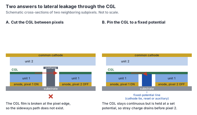
In this sample, the line of claims that ties the CGL to an electrode or a voltage numbers 7 at LG Display, 1 at Samsung Display (2016), and 3 among the five Chinese companies. All 7 of LG Display’s are still under examination in the US, so their final claim scope may still change.
5. How does latecomer China claim?
Mainland China’s tandem CGL patents began in December 2008 at a research institute, and among panel makers BOE first claimed one in December 2013. That is 10 years behind LG Display’s first CGL tandem claim (December 2003).
So China is now walking, all at once, the two stages Korea walked in sequence. Of the 124 tandem families among the five Chinese companies in 2021-24, 38 (31%) limited the CGL itself and 49 (40%) limited pixel structure. Over the same period, the CGL-itself share was 7% at LG Display and 12% at Samsung Display.
5.1 December 2008: two filings, two days apart
The Changchun Institute of Applied Chemistry, Chinese Academy of Sciences, filed on December 29, 2008 for a stacked organic EL device using an organic-semiconductor heterojunction CGL as the connecting layer (CN101447555B). The advantage its specification claimed was that this CGL is an undoped layer, simplifying the process. This patent lapsed after grant due to unpaid annuity fees.
Two days later, on December 31, Tsinghua University and Visionox filed for a structure with a specific compound in the connecting layer between units, co-doped with an alkali metal (CN101452997B). The specification states this connecting layer functions as a charge generation layer. It is the same family as Kodak’s n-type doping. This patent is still in force today.
After that, lighting company Haiyang Wang (海洋王照明) made its first filing in December 2010 and filed 96 in 2013 alone. These are for OLED lighting, not displays.
Among display panel makers, BOE claimed a CGL in a filing with a December 31, 2013 priority date (US9780323B2). It is a mixed conductive layer combining a material with conductivity above 10³ S/cm and one below 10⁻⁶ S/cm.
5.2 Themes Korea claimed first resurface years later
Among the claims by which the five Chinese companies limit the CGL itself, themes that Korea’s two companies claimed first reappear years later. The theme is the same; the claim is not.
| Theme | Korea (first) | China (later) |
|---|---|---|
| Splitting the n-type CGL host in two | LG Display US9065068B2 (2013) · two hosts of different LUMO plus a dopant | BOE US20240268142A1 (2022) · two electron-transport materials of different electron mobility plus a metal |
| Undoped p-type CGL | LG Display US8912534B2 (2012) · US10014357B2 (2016) | BOE CN121908770A (filed 2026) · an undoped p-type CGL with a strong electron-acceptor structure |
| Varying dopant concentration layer by layer | Samsung Display US20180114939A1 (2016) · concentration gradient | Visionox affiliate CN117460276A (2023) · two p-type CGL layers, with the second layer’s concentration lowered |
| Cutting the CGL at each pixel | LG Display US9721997B2 (2014) | BOE US11114636B2 (2017) and others; 32 families in 2021-24 with cutting/leakage language |
Of 56 US documents from the five Chinese companies, 37 carried LG Display patents in their citation lists. But only 6 were cited directly by the Chinese company itself; the rest were citations by a US examiner or by documents in the same family. On the same basis, Kodak appeared in 12 documents.
What can be said is only that the patent US examiners most often placed as prior art ahead of Chinese tandem patents is LG Display’s.
5.3 Directions not seen in Korean patents
Chinese claims also include directions not seen in this sample’s Korean-company patents.
- Solution-processed CGL: CSOT’s 2022 filing (US20240107787A1) claims a CGL material as a mixture of an n-type organic material, a p-type organic material, and a polar solvent. The specification states that because the emission layer uses a non-polar solvent, the n-type CGL above it must be deposited with a polar solvent so the layer beneath is not damaged. It targets a process of depositing the layer from solution
- CGL stacking for micro-LED: CSOT’s 2023 utility model (CN221008955U) links three micro-LED epi-wafers with two CGL layers, stacking them into a single subpixel. The specification states that in existing vertical stacking, the wiring process between epi-wafers damages the wafer. Chinese utility models do not undergo substantive examination
- Perovskite CGL: CSOT’s 2017 US filing (US20180315945A1) claims a CGL made entirely of an organic-inorganic perovskite, but it was abandoned in the US. Samsung Display’s perovskite CGL filing (July 2016) precedes it by nine months
6. What this analysis does not say
- Classification was done by one person. Reading the characterizing portion of claim 1, only a single primary limitation was chosen for each. In the random 48-document recheck, 85% agreed, and where it disagreed, the first classification had undercounted, slightly, both the CGL-itself and pixel-structure categories. No third-party verification was performed
- Korea was counted from US documents only. Patents filed only in Korea were left out. China was counted mixing US and Chinese documents, so counts are not compared between companies
- The search term is tied to the phrase “charge generation layer.” Semiconductor Energy Laboratory calls the same layer an “intermediate layer,” and Kodak also calls it an “intermediate connector.” Patents using only such alternate terms were left out of the population. Semiconductor Energy Laboratory’s 2012 patent was found by following citation relationships
- Citation is not endorsement. Most citations are added by examiners. They do not indicate imitation or influence
- Claims were placed side by side, but infringement or design-around was not judged. Whether the two companies’ claims fall within Kodak’s patent scope, or the relationship between Semiconductor Energy Laboratory’s patent and the later cutting structures, was not judged
- The enforcement or licensing history of the Semiconductor Energy Laboratory/Sharp patent was not investigated. That does not mean none exists
- LG Display’s 7 “potential-pinning” documents are all still under examination in the US. Claims may narrow upon grant
- Whether Samsung’s Penta Tandem product’s color composition matches the five-stack filing (US20230320120A1) could not be confirmed
- Why the shift from the 2013-16 peak toward the post-2017 direction happened cannot be established from patent documents alone. The specifications state only the background that “pixel spacing narrowed”
7. Conclusion
The way of linking emission units in a tandem OLED began with a metal conductor in 1997 and settled, in 2002, into Kodak’s n-type/p-type doped organic connecting layer. The patent most often placed as prior art ahead of Korea’s two companies’ tandem patents is also Kodak’s. That patent expired on April 26, 2022.
Within that framework, Korea’s two companies filed the most claims varying host count, presence of doping, and concentration distribution in 2013-16. After 2017 the weight shifted to pixel structure, and those specifications cite narrowed pixel spacing as the backdrop — the same ground as the lateral-conductivity problem Kido wrote about in 2002.
Facing the same leakage, Samsung Display claimed more structures that cut the CGL, while LG Display separately claimed structures that pin the CGL by connecting it to an electrode. China started with a research institute in 2008 and a panel maker in 2013, and now claims CGL refinement and pixel structure together. Themes Korea claimed first resurface years later, and China also opens directions not seen in Korean patents, such as solution processing and micro-LED.
The framework has been settled; what remains contested is where that framework is cut, and where it is pinned.