
LG Display's maskless patterning, FLiPP
LG Display unveiled FLiPP, which draws pixels without a metal mask, and put forward 1.6 times the luminance, 2.4 times the lifetime and a 13% cut in power. But those three figures do not come from a new emissive material. Feed in the single number of a 1.55-fold aperture ratio and all three fall out of arithmetic. After checking the sums, we read the foundational patent of this technology family. Samsung Display holds it now, and the place it aimed at was the exact opposite of LG Display's.
This article was published before the English edition began, so the labels inside its figures and simulators are in Korean. The caption and the note under each figure are in English.
This column gathers the display industry stories that poured out over one week (Monday to Sunday) and digs a little deeper into the hottest single issue among them.
Week 3 of August: the issues the press covered
The news filling the pages between 17 and 23 August fell into roughly six strands. This week what happened in Busan pushed all the rest aside.
First, IMID 2026 opened and closed. From 18 to 21 August, Korea’s largest display academic and exhibition event ran at BEXCO in Busan. Around 1,000 papers, some 80 booths and about 2,500 people. Samsung Display research head Sungchan Cho opened with a keynote on “AI and form factor innovation,” and Google and Meta also took the podium. What was a notice of an upcoming opening when the last issue went out became a real event this week.
Second, Samsung Display showed screens that stretch and twist. A 20-inch large-area stretchable display and a 7.6-inch wide-view display were shown as working units. Wide view is an optical technology aimed at the darkening and colour shift at the fold when a foldable is viewed from the side.
Third, Samsung Display secured cash. On 21 August a resolution was passed for Samsung SDI to sell back the 13,088,235 Samsung Display shares it held for 4.45 trillion won. From Samsung Display’s side it is a treasury share acquisition. In the same week came news of approval for framework construction of a new OLED plant at the Asan second complex in South Chungcheong. A building halted since 2021 goes up again.
Fourth, Apple widens OLED across the whole line-up. Reports repeated in the latter half of the week that after the iPad Pro, the iPad Air and mini, the MacBook Pro and Air, and even the all-in-one desktop iMac will get OLED over three years. For the iMac, Samsung Display’s high-density QD-OLED and LG Display’s 5-stack WOLED are under evaluation against a 220PPI and 600 nit requirement.
Fifth, only OLED grew in TV. Global TV shipments in the second quarter of 2026 fell 0.4% while OLED TV alone rose 20%. LG Electronics held a majority at 52%, and in LCD, Samsung Electronics at 13.7% and TCL at 13.8% were separated by 0.1%p. On the Chinese side, TCL acquired all remaining shares in its subsidiary CSOT, tidying the governance structure to 100%.
Sixth, the move to seize measurement standards first continued. The Korea Display Industry Association held an International Committee for Display Metrology (ICDM) meeting and an international standards forum in Busan, beginning work on IDMS 1.4, the next-generation metrology standard. Foldable crease measurement, automotive slidable and curved optical evaluation, and XR microdisplay luminance measurement are the subjects.
Running through all six strands was one story that did not miss a single day of the week, and it was not about screens but about how screens are made.
The hottest issue of week 3 of August is “LG Display FLiPP.”
The mask is gone, so why is lifetime the news?
The technology LG Display unveiled on 18 August is called FLiPP, the initials of FMM-Less innovative Pixel Patterning, a process that draws red, green and blue pixels without a fine metal mask (FMM).
FMM is the method used to make OLED pixels for close to 30 years. A thin metal sheet perforated only where wanted is pressed against the glass substrate, and organic material is evaporated over it so that only what passes through the holes accumulates. The principle is the same as spraying through a stencil. The problem is that this metal sheet has to be thin, and a thin sheet sags. When it sags the organic material lands in the wrong place. The analysis of nine Gen 8.6 OLED deposition and mask patents in this same issue is about exactly that sag.
So the word that always followed talk of removing the mask was resolution. No mask, no sag; no sag, smaller pixels.
And yet the number LG Display led with in this announcement was not resolution.
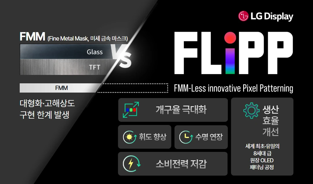
Four figures were announced.
| Item | What was announced |
|---|---|
| Aperture ratio | about 55% higher than the FMM approach |
| Luminance | 1.6 times |
| Lifetime | 2.4 times |
| Power consumption | 13% lower |
| Glass utilization | 64% higher panel yield from a Gen 8.5 mother glass |
Youngsuk Choi, LG Display’s chief technology officer, said the company “concentrated its proprietary WOLED technology and know-how to succeed in realizing FLiPP, the next-generation OLED patterning called the dream technology.”
The 2.4 times lifetime is the most striking number on the list. In OLED, lifetime has been treated as a materials problem. The reason blue phosphorescence went nearly 20 years without commercialization was lifetime. And here a process change is said to have made lifetime 2.4 times.
There is one thing to ask. Where did that 2.4 come from?
All three figures come from the aperture ratio alone
The answer is at the top of the list. Aperture ratio.
Aperture ratio is the fraction of the area a pixel occupies that actually emits light. The rest is taken by the banks and wiring separating pixels from one another. According to Byungsoo So, executive at Samsung Display, in March this year, the aperture ratio of the FMM approach is around 30%. Only a third of the pixel area emits.
The aperture ratio is low in the FMM approach because the mask has thickness. Where a hole has walls, those walls block obliquely arriving organic material and leave a deposit smaller than the hole. This is called the shadow effect. So the holes have to be spaced generously at the design stage, and all of that margin becomes non-emitting area.
FLiPP recovers that margin. Take the 55% improvement LG Display stated at face value and the aperture ratio becomes 1.55 times.
Now put the other three figures against it one by one.
Luminance. Driven at the same current density, total light output is proportional to the emitting area. If the area is 1.55 times, the light is 1.55 times. The announced value is 1.6 times. Essentially the same.
Lifetime. OLED lifetime is set by how hard the device is driven. The literature writes the relation between lifetime τ and current density J as a power law.
τ ∝ J−n
The exponent n runs roughly between 1.5 and 2.0 depending on device structure and the carrier concentration dependence of mobility, and 1.7 to 1.8 is commonly used for converting to initial luminanceSince the emitting area is 1.55 times, making a screen of the same brightness means driving each pixel only 1/1.55 as hard. Current density falls to 1/1.55. Lifetime then goes as 1.55 to the power n.
Take n as 1.7 and it is 2.11 times, 1.8 gives 2.20 times, 2.0 gives 2.40 times.
Solve backwards for the n that produces the announced 2.4 times and it comes out at exactly 1.998. The 2.4 times lifetime is the square of the 1.55 times aperture ratio.
Power consumption. This is in fact the decisive evidence for the reading. The first two figures jumped, and yet power fell only 13%. It looks inconsistent at a glance, but work it out and this is the part that fits.
If the emitting area becomes 1.55 times and current density falls to 1/1.55, the product of the two, the total current, is unchanged. Power is voltage times current, so with total current unchanged the only route by which power falls is the drive voltage. Drive voltage does fall as current density falls, but not by as much. So a 55% rise in aperture ratio cuts power only by around 10%.
Set the built-in potential at 1.5V and the reference drive voltage at 4.0V and the calculation gives a 12.3% reduction. Almost the same as the announced 13%.
Move the sliders and it is immediately visible that the three values are bound into one. Hold the aperture multiple at 1.55 and raise only the lifetime exponent n from 1.4 to 2.2, and the lifetime bar swings between 1.9 and 2.6 times, touching the announced 2.4 times, marked by the dashed line, when n is 2.0.
In short: the luminance, lifetime and power figures FLiPP put forward are not the achievement of a new emissive material but the result of widening the pixel. Leave the emissive layer as it is and widen only the emitting area, and the three values follow on their own.
This is not a flaw. If anything it says precisely what this technology changes. FLiPP is not a technology that changes the material but one that widens the space the material sits in. And widening the space is far faster than changing the material. Blue phosphorescence took 20 years; LG Display says it took about one year to settle FLiPP’s process conditions.
Why doesn’t the organic material dissolve when it is dipped in solvent?
The process LG Display described runs like this. Red, green and blue pixels are coated onto the substrate in turn and fixed in exact position, and ultraviolet light erases what is not needed. The detailed conditions have not been disclosed.
Read it and one part catches immediately. The erasing. How do you erase organic material?
An OLED’s organic layers are around 100 nanometres thick and weak to heat, moisture and solvent alike. The ordinary photoresists used in semiconductor processes take strong organic solvents or alkaline developers, and dip an OLED in those and it is finished on the spot. The reason maskless patterning went unrealized for 30 years was not precision but this.
The answer is chemical orthogonality. Most organic semiconductors are friendly either to oil or to water. Highly fluorinated compounds mix with neither. They are orthogonal to both. So with a fluorinated photoresist and a fluorinated developer, the liquid washes away only the resist without touching the organic layer beneath.
The company that developed this approach was named Orthogonal Inc. The company name was the principle.
LG Display described FLiPP as proprietary and did not mention Orthogonal. But what problem this family of technologies solves, and how, is set down without omission in the granted patents Orthogonal left behind. So we read them.
The patent does not dissolve and wash. It floats away
Granted patent US10,468,637 is titled “Color OLED display with a larger aperture ratio.” The patent title already says that the purpose of removing the mask is not resolution but aperture ratio. The priority date is 1 August 2014, eight years before JDI announced eLEAP.
The method this patent uses does not expose or develop the organic material directly. The order is the reverse.
First an undercut lift-off structure is built on the substrate. There is a hole wherever a pixel will sit, and the hole walls are cut inward into an eave shape. Organic material is then deposited over the whole thing. What enters the hole lands on the substrate; what settles on the eaves remains, cut off from below. Dipping in a fluorinated solvent then dissolves the eave structure, and the organic material resting on it comes away with it. Only what sits inside the holes remains. This is repeated three times for red, green and blue, and a common upper electrode goes on last.
One condition the patent’s embodiments require stands out here.
The effective density of at least one lift-off structure combined with the organic EL layer and upper electrode layer above it is less than the density of the lift-off liquid used to remove that structure.
US10,468,637 embodiments 7 and 27It means the density is designed so that the detached piece floats rather than sinks. Another embodiment writes that the structure “curls” during removal, and another selects materials so that it “at least partially curls up and floats away from the substrate.”
That is the core of this technology. The organic material is not dissolved and washed away; the sacrificial layer carrying it is rolled up whole and floated off on the liquid. The organic material meant to stay sits inside the holes under the eaves, exposed to the flow only briefly.
The material conditions are specific too. The fluorinated underlayer is a methacrylate fluoropolymer of about 49 weight percent fluorine, dissolved at about 12 weight percent in a hydrofluoroether solvent, spin coated at 3,000rpm for 1 minute and baked at 90 degrees for 1 minute. The thickness is about 800 nanometres. The patent notes that this underlayer must be at least 100 nanometres thicker than the height of the dielectric pattern beneath for lift-off to work properly. Hydrofluoroethers such as HFE-7100 and HFE-7300 are named as lift-off agents.
And the current owner of this patent is not Orthogonal. It was assigned to Samsung Display on 10 June 2024. There were reports that Samsung Display bought five US patents from Orthogonal and two Korean patents in 2025; that transaction is right there in the patent register.
The place the patent aimed at was not large area but high resolution
Read the patent to the end and it becomes clear where this technology originally aimed. And that place is not the 27-inch panel LG Display stood in its booth.
Embodiment 1 of the patent is a record of something actually made. A dielectric was patterned about 500 nanometres thick on a glass substrate, and pixel apertures were opened 10 micrometres across and 36 micrometres high. Different colours were spaced 4 micrometres apart, the same colour 6 micrometres. One red-green-blue set fits in 40 micrometres by 40 micrometres.
Convert those dimensions and you get 635dpi at 61% aperture ratio.
The scope the patent claims points the same way.
| Embodiment | Content |
|---|---|
| 84 | pixel spacing 4μm or less, combined emitting area 60% or more of the display region |
| 88 | aperture ratio above about 60% and also resolution above 600ppi |
| 89 | aperture ratio above about 70% |
| 90 · 91 | resolution above 700ppi · above 800ppi |
| 92 to 95 | pixel size under 25μm · 15μm · 5μm in any direction |
What matters here is that number 88 binds aperture ratio and resolution into a single condition. In the FMM approach the two eat each other. Raise the resolution and the pixel shrinks, but the margin that must be left empty because of mask shadow does not shrink as much. So the higher the resolution, the more steeply the aperture ratio falls. That is why the aperture ratio of FMM panels for smartphones sits around 30%.
Maskless breaks that conflict. Because the margin is set by lithography rather than the mask, shrinking the pixel shrinks the margin with it. Which is how a combination of 61% at 635dpi holds.
Lay this announcement over that passage and the picture changes.
| Orthogonal patent (2014-2015) | LGD FLiPP (2026) | |
|---|---|---|
| Resolution | 635dpi (measured, embodiment 1) | about 163ppi at 27 inches |
| Aperture ratio | 61% | about 46.5% converted from 30% |
| Aimed at | high-resolution small | large-area Gen 8.5 full glass |
LG Display is not yet using this technology’s greatest strength. What maskless is originally good at is placing small pixels densely while still making them bright, and what LG Display proved first was processing a large sheet of glass in one piece. That is also why the aperture ratio improvement came out lowest of the three. In large area there was less room to raise it in the first place.
And that explains why Samsung Display bought this particular patent. Samsung Display’s mainstay is high-resolution panels for smartphones, and XR microdisplays are denser still. A right claiming 60 to 70% aperture ratio above 600ppi belongs precisely to that market.
Two companies took opposite ends of the same technology. LG Display went toward growing the glass, Samsung Display toward shrinking the pixel.
An aperture ratio of 46%, the lowest of the three
LG Display called FLiPP a “world first.” It is worth confirming exactly what that phrase attaches to, because drawing OLED pixels without a mask is not itself a first.
Japan’s JDI announced eLEAP in 2022, and China’s Visionox has already produced mass-production samples with ViP. Put the three companies’ announced figures side by side on aperture ratio and it looks like this.
| JDI eLEAP | Visionox ViP | LGD FLiPP | |
|---|---|---|---|
| Announced | May 2022 | 2023 | August 2026 |
| Aperture ratio | 28% → 60% (2.14 times) | 29% → 69% (2.38 times) | 1.55 times vs FMM |
| Converted from 30% | 64.2% | 71.4% | 46.5% |
| Luminance | 2 times | 4 times | 1.6 times |
| Lifetime | 3 times | 6 times (with tandem) | 2.4 times |
| Back-solved exponent n | 1.44 | 2.07 | 2.00 |
| Mother glass | Gen 6 | Gen 6 · Gen 8.6 (2027 target) | Gen 8.5 full glass |
On aperture ratio improvement alone LG Display is lowest of the three. Converted on the same basis it is 46.5%, short of JDI’s 64.2% and Visionox’s 71.4%.
This table must not be read straight as a ranking, though, because the three companies are measuring different things. JDI speaks on a basis of 300PPI, Visionox up to 1,700PPI. Both are smartphone and XR pixel densities. The smaller the pixel, the larger the share taken by banks and wiring, so the FMM aperture ratio is near the floor, and a low floor leaves large room to rise. What LG Display showed in its booth, by contrast, was a 27-inch monitor. A 27-inch 4K panel is around 163PPI, and at that size FMM already gives a fairly high aperture ratio. A large denominator makes the multiple small.
The trouble is that LG Display disclosed neither the absolute aperture ratio nor the pixel density of the FMM panel used as the comparison. The figure of 55% alone cannot tell us whether it raised 30% to 46% or 45% to 70%. Until that value is released, placing the three companies’ aperture ratios in one table and ranking them is impossible.
Why Gen 8.5 rather than Gen 8.6?
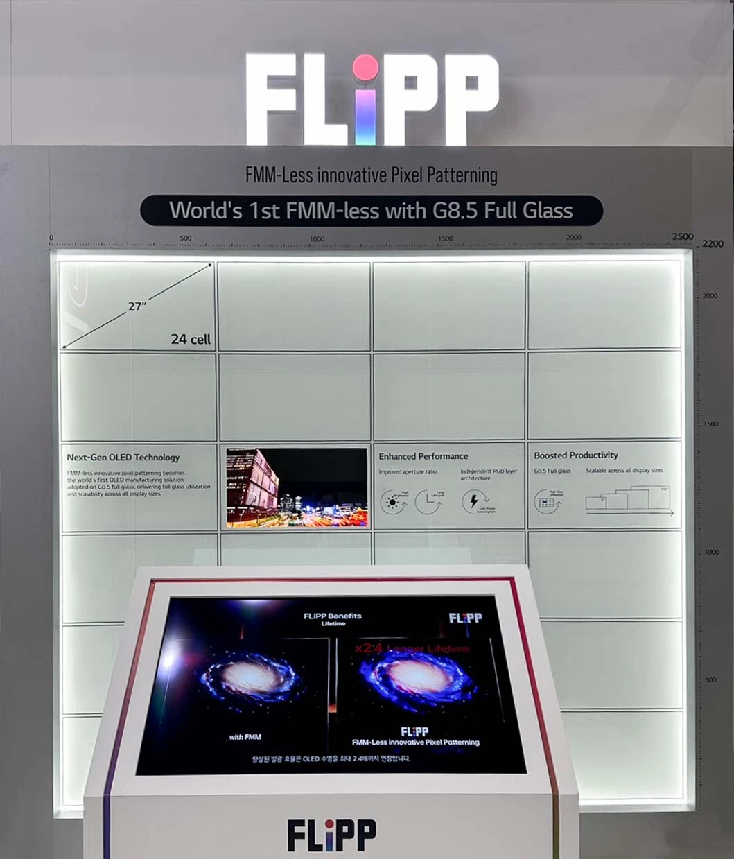
So where does “world first” attach? The line at the top of the booth answers. “World’s 1st FMM-less with G8.5 Full Glass.” Not maskless as such, but being the first to use a Gen 8.5 mother glass whole, as one piece.
This is not a passage to skip past. The lines the industry is currently building for IT OLED are all Gen 8.6. Samsung Display put in 4 trillion won, and Visionox is raising a 7.6 billion dollar Gen 8.6 V5 line in Hefei. And yet LG Display said Gen 8.5.
Connect two things and the reason appears. First, LG Display has not yet decided on Gen 8.6 IT OLED investment. It has held to a stance of “no investment without a customer” for several years, serving the medium-size market with Gen 6 lines. Second, LG Display already has a Gen 8.5 large-area line, the one making WOLED for TVs.
That is, FLiPP is both an image-quality technology and an answer about investment scale. If IT-grade RGB OLED can be made at the existing sheet size without building a line of a new generation, then deferring Gen 8.6 investment becomes a different route rather than falling behind.
The numbers written in the booth support this reading. On a Gen 8.5 sheet of 2,500 by 2,200mm, a cutting layout of 24 panels of 27 inches was drawn. We checked whether it actually fits.
A 27-inch 16:9 panel is 597.7mm by 336.2mm. Divide the sheet into 4 columns and 6 rows and each cell is 625.0 by 366.7mm, leaving a margin of 27.3mm across and 30.4mm down after the panel goes in. Sensible values for cutting clearance. 24 fit exactly. The panels then occupy 87.7% of the sheet’s 5.50m² area.
Cut the sheet in half and this number cannot arise. One more cutting line appears and each half needs its own edge margins again. Given that the reason the FMM approach uses half glass at Gen 8.6 is that a mask cannot be made at full sheet size, it also becomes clear that the announced “64% higher panel yield” is a separate story from aperture ratio. One is area inside the pixel, the other area on the glass.
The basis for the 64%, however, was not disclosed by LG Display. Which generation and which cutting conditions it was compared against remains unreleased.
What this process pays
One thing absent from the announcement has to be raised.
Maskless patterning repeats the same process three times, for red, green and blue. The process flow chart in the Orthogonal patent draws that repetition exactly. Form the lift-off structure, clean residues, deposit the organic layer, deposit the upper electrode, remove the lift-off structure. Those five steps run three times, and the common upper electrode goes on at the end.
Which means the layer of the colour laid down first goes through the whole process of the other two colours again. The first colour passes chemical processing three times, the second twice, the last once.
That a fluorinated solvent does not dissolve the organic layer and that it leaves no trace at all are different statements. Each pass through the process can leave trace moisture and residual solvent at the interface, and if that quantity differs by colour, the three colours start out with their degradation rates already mismatched. A screen’s colour balance holds only while the three colours darken at the same rate. Whites drifting toward one colour with long use can arise here.
The grounds for saying this is not speculation are in the patent itself. Orthogonal designed with this problem in mind. The patent cites, among its references, an SID 2014 presentation on extrinsic degradation of phosphorescent OLEDs, and its embodiments separately include a condition that the upper electrode be deposited so as to cover even the sidewalls of the organic layer, and a condition that a layer of material less sensitive to water and oxygen be laid on to protect the organic layer beneath. Which is to say that how to wrap the earlier layers while the process goes round several times was a design problem of this technology.
How LG Display handled this has not been disclosed. But where the industry sees this family’s weakness is on record. Introducing non-FMM technology in March this year, Samsung Display executive Byungsoo So said there are “problems in production yield and encapsulation reliability,” adding that “no technology has yet reached the mass production stage.” Encapsulation is the layer that shields the organic layers from moisture and oxygen. The very place the patent says to cover down to the sidewalls is what a competitor’s executive named as an unsolved problem.
That what stood in the booth was a 27-inch monitor points the same way. At 27 inches the pixels are large, the most forgiving condition for this process. That LG Display named tablets and monitors as its mass-production starting point is likely for the same reason.
Outlook
FLiPP is the thing it was announced to be. But the account of what it is has to be read a little differently from the announcement.
This technology’s achievement is not a new emissive material. Luminance 1.6 times, lifetime 2.4 times, power down 13% all fall out of arithmetic once the single figure of a 1.55 times aperture ratio is fed in. And that fact does not diminish the technology’s value. In an industry where changing a material takes 20 years, it secured a route to the same result by widening the space, in one year.
Three predictions.
First, LG Display goes the way of not building a new Gen 8.6 IT OLED line. Announcing that FLiPP was demonstrated on Gen 8.5 full glass is itself a signal in that direction. Whether this prediction holds will be confirmed by whether Gen 8.6 investment is executed at Paju P10. If an investment decision comes within the year, this reading is wrong.
Second, the non-FMM Samsung Display brings out will be high resolution, not large area. The Orthogonal patent it bought claims 60 to 70% aperture ratio above 600ppi, and what its embodiment measured was a 635dpi panel. That it agreed to take a vertical deposition tool for non-FMM from Applied Materials also runs differently from a large-sheet process. If Samsung Display comes out with Gen 8.5 glass using this technology, this prediction is wrong. The observation points are next year’s SID Display Week and IMID 2027, and the number to watch is not glass size but ppi.
Third, whoever discloses the absolute aperture ratio together with the pixel density takes the next round. Right now the three companies quote only multiples on different bases, making comparison impossible. Yet this technology’s worth lies not in aperture ratio alone but in the combination of aperture ratio and resolution. That is why the patent bound the two into a single condition when claiming its right. Those who actually buy panels, like Apple, have no choice but to demand both numbers rather than a multiple. The moment those numbers are released, the table in this article has to be redrawn.
One last thing. The surest fact in this announcement is neither lifetime nor luminance. It is that removing the mask has come out of the laboratory after 30 years. JDI opened the door in 2022, Visionox followed with mass-production samples, and LG Display pushed it onto large sheets. If three companies have each moved in the same direction at different sizes, that is not one company’s choice but the industry’s direction.