
The driver IC bottleneck sits on UMC's 22nm line
Two driver IC stories landed in the same week. Samsung Display said it had moved the driver IC for its new panel from 28nm to 22nm, and Samsung Electronics pushed 10% of its Galaxy Z Fold8 component production plan to the following month because driver ICs were short. Both stories point at the same 22nm. What decides when panels get better turned out to be not the panel fab but the room left on a mature node foundry line.
Hot Issue of the Week
This column gathers the display industry stories that filled one week (Monday to Sunday) and digs a little deeper into the single hottest one.
The stories the press ran from 14 to 20 September
This week an event and a component split the pages between them. The 17th Display Day was held on 17 September, and panel records and supply chain news lined up before and after it.
First, Samsung Display unveiled a smartphone OLED that puts 165Hz on top of 2K resolution on 14 September. It goes into the iQOO 16, which vivo’s gaming brand iQOO is launching this month. It is 6.9 inches, and the company said power consumption is about 30% lower than in the previous generation.
Second, in the same week Samsung Electronics pushed 10% of its component production plan for the Galaxy Z Fold8 to the following month because driver ICs were short. It is tens of thousands of units out of the several hundred thousand planned for September.
Third, the 17th Display Day was held in Seoul on 17 September. The Silver Tower Order of Industrial Service Merit went to Lee Ki-seung, chief executive of Sekyung Hi-Tech, which localised foldable optical film. The government presented a roadmap aimed at 2040 and a target of 80% localisation for materials, parts and equipment.
Fourth, LG Display has begun joint development of an OLED for fighter jet cockpits with Hanwha Systems. This is a position that imported high-reliability LCD has held until now. It is an attempt to extend tandem OLED beyond automotive into aviation and defence.
Fifth, investment in microdisplays continued. Samsung Display decided to invest about 300 billion won in an RGB OLEDoS line based on 12-inch silicon wafers, with mass production targeted for 2028. Sony, Seeya and BOE currently hold more than 90% of the OLEDoS market.
Sixth, there was news on a patent dispute and on panel prices. Samsung Display filed for invalidation of three CSOT patents with the US Patent Trial and Appeal Board on 17 September, and the three Chinese panel makers decided to raise TV panel prices in September and October.
Of these, dual UTG and the foldable shipment outlook, chipflation, and the Asan A7 plant were already covered through the previous issue, so they are not opened again here.
The hottest issue from 14 to 20 September is “the display driver IC (DDI).”
Two stories point at the same 22nm
The driver IC (DDI) is the chip that decides what voltage to put into each pixel of a panel and delivers it. Between 14 and 20 September, news about this component came out twice, and the two pointed in opposite directions.
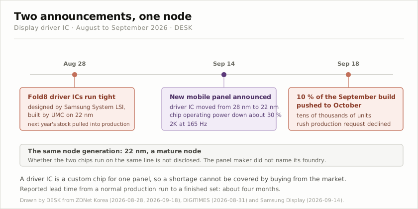
On 14 September, in unveiling a new mobile panel, Samsung Display said it had moved the driver IC process from 28nm to 22nm. The explanation added that the power the chip uses for computation has been cut by about 30%.
Four days later, on 18 September, reports said Samsung Electronics had pushed 10% of its component production plan for the Galaxy Z Fold8 to October because of a driver IC shortage. It is tens of thousands of units out of the several hundred thousand set for September.
This is where the two stories meet. According to the reports, the driver IC that goes into the Fold8 is designed by Samsung Electronics’ System LSI and made by Taiwan’s UMC on a 22nm process. That is the same node as the process the new panel moved to.
One thing should be made clear, however. Whether the two chips use the same production line has not been disclosed. Samsung Display did not say which foundry makes the driver IC for this panel. What can be confirmed goes only as far as the fact that the two products use the same node generation.
The weight of the material this article stands on should be stated up front as well. The panel announcement and the foundry results are materials the companies issued themselves, while the Fold8 production deferral and the refusal of a rush order are reports citing industry officials. And the reading that the two sets of demand collide in the same place is a judgment built on top of that.
Why it is 22nm that gets blocked
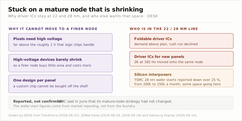
Because the driver IC is a component that cannot run away to a finer process. Turning a pixel on means generating and delivering a voltage far higher than the 1V or so that logic chips handle. High-voltage devices do not shrink well as the process scales down, so driver ICs stay on mature nodes such as 28nm and 22nm.
Driver IC supply therefore moves independently of expansion at the leading edge. However much a foundry invests in 2nm, the space a driver IC can use does not grow.
One more property is attached here. A driver IC is a custom chip built to match the pixel count and the drive scheme of each panel. It cannot be bought off the market the way memory can, and when it runs short the volume dedicated to that product has to be made again.
According to the reports, Samsung Electronics asked UMC for a rush run (super hot run) and was turned down. The answer was that UMC’s 22nm line is already full with products for several customers, so the schedule cannot be pulled forward.
So the two cards Samsung Electronics actually played were these. It turned driver IC volume secured for next year’s product development over to mass production, and it drew on remaining inventory as far as it could. The reports said that going through normal production to a finished product takes about four months.
The claim that the line is full also appears in an earnings release
The supply story so far comes from reports citing industry officials. But the second quarter 2026 earnings release UMC issued carries numbers pointing in the same direction.
That release led with “third quarter utilisation above 90%” in its very headline. Second quarter utilisation was 85%, and wafer shipments rose 10.6% from the previous quarter.
Node by node it is clearer. 22nm and 28nm accounted for 37% of wafer revenue, and 22nm alone was 17.5% of second quarter revenue, an all-time high. Chief Executive Jason Wang said the 22nm and 28nm business keeps setting records.
In the same release the company said its 12-inch capacity is already at healthy utilisation, approved an expansion of its Singapore fab and the construction of a new fab in Tainan, and raised its 2026 capital expenditure budget to $2 billion. It decided to add capacity because there is no room.
To sum up: how the Fold8 volume came to slip is a report and not a fact the company has confirmed, but the “full 22nm” that the report describes does not contradict the foundry’s disclosed figures.
Mature nodes are not growing, they are leaking away
If the ground the driver IC stands on were widening, time would loosen this bottleneck. The direction, however, is the opposite.
TrendForce reported on 22 June that TSMC has cut 28nm wafer input by more than 25% since the start of 2026. Input that stood at around 200,000 wafers a month came down to 150,000, and part of the space freed up went to silicon interposer production.
An interposer is the wiring layer laid underneath when several chips are mounted in one package. AI accelerator demand is taking this space, and it is also the space that the glass core substrate covered in the fifth issue is aiming at.
In other words, the driver IC is tied to the mature node, and that mature node is moving toward advanced packaging. It is not that displays are being pushed out of semiconductor processes, but that the order of priority inside semiconductors is changing.
One qualification has to be attached. TSMC denied, at that same point in June, that it had changed its mature node strategy. The drop in wafer input is a figure carried by reports, not a policy the company has confirmed.
Still, the disclosed figures point the same way. In TSMC’s second quarter 2026 results, 28nm accounted for 6% of total revenue, while leading-edge processes of 7nm and below took about 77%. In the same quarter, revenue from 45/40nm, 28nm and 16nm all fell from the previous quarter.
So how much wafer input actually fell is not confirmed, but the fact that the place mature nodes hold in this company’s revenue is getting smaller is confirmed by disclosure.
Do more foldables need more driver ICs
What the reports confirm goes only as far as the fact that demand exceeded expectations. The same reports said demand for the Fold8 ran above plan, so that even volume held for next year’s development was drawn on, while the Flip8 is falling short of expectations.
Manufacturers do not disclose how many driver ICs go into one foldable. Since the large folding screen and the outer screen each have to be driven, it is natural to see the load as heavier than on a bar-type phone, but public materials give no basis for asserting a count.
What is certain is the direction. As foldables increase and resolution and refresh rate rise, driver ICs get either bigger or more numerous. When a chip gets bigger, the number that comes out of a single wafer falls, so the same capacity makes fewer of them.
Moving to 22nm actually creates more room
Shrinking the process reduces the area one chip takes, so more of them are cut from the same wafer. Moving from 28nm to 22nm is not only a choice that cuts power but also a choice that draws more chips out of the same capacity.
A wafer is round and a chip is rectangular, so part of the edge is thrown away. When the chip gets smaller this loss shrinks with it, and the count per wafer rises slightly more than the ratio by which the area fell.
But the place that is blocked right now is that very 22nm. The place it moved to in search of headroom was an already crowded line. Even if moving node raises the count per wafer, the total stays the same unless the number of wafers allocated on that line goes up.
Neither the driver IC’s actual dimensions nor how much area this transition removed has been disclosed. So the calculator below leaves those values open as sliders. It is a tool for seeing how much chip size changes the count per wafer, not for deciding which number is the answer.
The cards Samsung can play
First, widening the supplier base. DIGITIMES reported on 7 August that Samsung Electronics had approached Taiwan’s Novatek about driver ICs for the Galaxy S28 Ultra. Design and qualification take time, so it is not a means of filling the immediate shortage.
Second, changing foundry. When a custom chip moves process, the design has to be qualified again. The production period of about four months seen earlier is added on top of that once more.
Third, adjusting the product mix. This means putting volume first into the Fold8, where demand has gathered, and pushing the weaker-selling model back, and this deferral does in fact look close to that.
All three move on a quarterly timescale. It is hard to see this shortage being resolved within the year.
One more foldable arrives in the same quarter. Apple’s iPhone Duo goes on sale on 23 October, and Samsung Display supplies its panel. But who makes the driver IC for the iPhone Duo, and where, has not been disclosed, so whether it overlaps on the same 22nm space is not confirmed.
Outlook
We think the bottleneck that sets the pace of panel technology has moved outside the panel. New panels keep coming out with higher resolution and refresh rates, but the chips that drive them are tied to a mature node, and that node is not growing. The distance between announcement and mass production widens in this stretch.
So the place to watch from here is not panel announcements but driver IC supply plans. Three things to check are set down here.
First, will the volume pushed to October actually come out in October? If the reports are right, this volume is reflected in fourth quarter results. If it slips again, it means the bottleneck is not a one-quarter affair.
Second, will Novatek or another supplier turn into an actual order? Being in talks and being adopted for mass production are different things. If adoption is confirmed, Samsung Electronics has changed a structure that leaned on System LSI alone.
Third, where does the driver IC process of newly announced panels go? If 22nm is already a full space, the next generation of panels has to answer either by pushing more into the same node or with a design that cuts chip area. Whether a process number appears again in the announcement is the signal.