
Glass Core Substrate (GCS): AUO and Corning take on semiconductor packaging substrates
A panel company came out holding a semiconductor substrate. It is true that both the glass composition and large-area handling were made by display first. Yet the volume production schedules of all three companies have slipped, and working back from the via density written into the patents, the 40% yield the industry calls low already means succeeding at a single via 99.9964% of the time. The large area that was the reason for choosing glass is cutting that yield directly.
Hot Issue of the Week
This column gathers the display industry stories that filled one week (Monday to Sunday) and digs a little deeper into the single hottest one.
The stories the press ran from 31 August to 6 September
Two trade shows overlapped this week. SEMICON Taiwan ran in Taipei from 2 to 4 September and IFA opened in Berlin on 4 September, and in between the Omdia Korea Display Conference ran for two days in Seoul. News out of those three filled most of the week’s pages.
First, IFA 2026 was the thickest strand. Samsung Electronics opened Samsung Connect at Berlin’s Humboldt Forum and showed the Galaxy Z Fold8 Ultra, 4.1mm thick with a 193.2mm OLED in a 4:3 ratio, along with the 32-inch 4K 240Hz Odyssey OLED G8 and the 49-inch curved G9. LG Electronics brought out the 9mm-thick wireless Wallpaper W6 OLED TV and the third-generation Alpha11 AI processor. TCL showed the 32-inch OLED+ 32X3A that switches between 4K 240Hz and FHD 480Hz, and Hisense answered with 116-inch mini LED.
Second, the Omdia Korea Display Conference ran on 3 and 4 September in Yangjae, Seoul. Omdia put large OLED shipments this year at 38.8 million units, up 18.8% on the previous year. That figure comes while the TV market as a whole shrinks 2.5%. General manager David Hsieh warned that China could overtake Korea in mobile and IT OLED capacity by 2028, and director Jinhan Park expected Apple to split its next MacBook Pro into LCD and tandem OLED models because of the sharp rise in memory prices.
Third, Apple’s foldable announcement is close. With it expected around 10 September, forecasts of gains for the domestic FPCB and module value chain followed, and the world foldable phone market this year was put at 26.1 million units.
Fourth, on the materials side there was news of SFC’s listing. A blue emitter material specialist, it has Samsung Display holding 33.9% as second-largest shareholder. It is pursuing a KOSPI listing in November.
Fifth, LG Display moved onto a track for an annual operating profit of 1 trillion won and opened second-half R&D graduate hiring for the first time in four years. This comes after completing the sale of its large LCD operation in Guangzhou.
Sixth, on core technology, Professor Soo-Seok Choi of Ajou University received September’s Scientist of the Month award. The technology produces full colour from a single pixel using nano optical structures alone, without splitting into RGB subpixels. It touches the pixel density limit of microdisplays and is worth a separate piece of its own.
Of these, LG Display’s FLiPP, the slowdown in Chinese capital spending, KCC Glass entering OCA, and the 24.5-inch esports panel have all been covered through previous issues, so they are not opened again here.
The hottest issue from 31 August to 6 September is the “glass core substrate (GCS).”
A panel company stood in Corning’s booth holding a semiconductor substrate
At SEMICON Taiwan 2026, AUO showed a glass core substrate (Glass Core Substrate, GCS) in physical form. AUO is a large panel maker in Taiwan. A company that made LCDs for TVs and notebooks came out holding a semiconductor packaging substrate to carry AI server processors.
The press release AUO issued on 31 August states its grounds in a single line: it is developing this technology “on more than 30 years of expertise in handling glass substrates.” It said it is working through large-area glass processing, precision metallisation and redistribution layer (RDL) technology, and moving in turn through through-glass via (TGV) formation, via metallisation and reliability verification.
Read that announcement precisely, though, and what AUO is actually bringing separates out. GCS combines Corning’s semiconductor-grade glass with AUO’s RDL process, and the display was not in AUO’s own booth but in Corning’s booth. That is, the glass itself comes from Corning, and what the panel company brings is the technology for drawing circuits on glass.
Why that is a natural pairing shows up when the two processes are set side by side. Display makes TFT arrays on large-area glass. A glass core substrate makes redistribution layers on large-area glass. Putting fine wiring on a sheet, they are the same family of technology.
Semiconductors turned to glass because silicon is locked at 300mm
Start with the semiconductor side. As chiplet design became mainstream, several chips ended up on one package, and that requires bigger substrates and denser wiring. There were two existing options.
Organic substrates have improved thermal expansion and glass transition temperature with fillers, but they have limits in thermal stability, flatness and dimensional stability. Especially as area grows. Thickening the core to reduce warpage then makes it harder to make small through-holes.
Silicon interposers can carry fine wiring using semiconductor back-end technology, and their thermal expansion matches the chip so warpage is small. But transmission loss is high, which makes high-speed signalling difficult, and because they are made on 300mm wafers, substrate size and yield are tied together. So they are expensive.
Glass sidesteps both problems at once. Flatness, thickness uniformity, dimensional stability and stiffness are good, and the coefficient of thermal expansion can be tuned, so warpage can be held down even when thin. Dielectric loss is low, which suits high-frequency signals. And as the IEEE Electronics Packaging Society technical document puts it, glass “can be manufactured in large panel form like display substrates.”
The numbers make the difference clear. Silicon interposers are made on 300mm-diameter round wafers, while for glass a 650mm × 550mm TGV substrate has already been reported in the literature. By area that is 706.9cm² against 3,575cm², 5.06 times. And one more thing follows. Cutting rectangular packages from a round wafer throws the whole edge away, while a rectangular panel has no such loss. In a world where cost is set by how many you take out of the same equipment in one pass, that difference becomes cost directly.
| Organic | Silicon | Glass | |
|---|---|---|---|
| Flatness, thickness uniformity | Poor | Good | Good |
| Stiffness, dimensional stability | Poor | Good | Good |
| CTE tunability | Possible | Difficult | Possible |
| Permittivity, dielectric loss | Good | Poor | Good |
| Thermal conductivity | Poor | Good | Poor |
| Large-area panel | Possible | Wafer only | Possible |
| Process maturity | Mature | Mature | In development |
The last row of the table is worth a close look. Glass is good on almost every item, and only the one row for process maturity says “in development.” The same document puts it more plainly in the body text: “Glass is not yet commercialised and needs further development.” That sentence is from November 2025.
What carried over, one: the glass composition itself is something display made
The glass used in semiconductor packaging is not just any glass. It is alkali-free glass.
Display made this composition. Because alkali ions in glass ruin the semiconductor behaviour of thin-film transistors, putting TFTs on glass required glass with alkali oxides held below 0.1%. As LCD went into volume production, this glass came to be made at industrial scale.
The glass used for the TGV experiment in the IEEE document cited above is EN-A1. It is AGC’s alkali-free alumino-borosilicate glass, with a coefficient of thermal expansion of 3.8ppm/K and standard thicknesses of 0.3mm, 0.5mm and 0.7mm. It is matched close to silicon’s 3.2 to 3.3ppm/K, and the thicknesses are the same specifications display substrate glass has always used. AGC sells this glass both as thin strengthened glass for displays and as interposer glass for TGV, wafer-level packaging and MEMS. It is the same product.
The lineage is in the document itself. The author of this IEEE technical paper is from AGC’s advanced semiconductor packaging group, and the reference cited where it deals with glass fracture is an Asahi Glass research report. Corning, AGC and Nippon Electric Glass, which supplied LCD substrate glass, stand as the semiconductor glass substrate suppliers unchanged.
What carried over, two: how to drill the holes
To use glass as a substrate you have to drill holes connecting top and bottom. Through-glass vias, TGV. The target is under 200μm in diameter, and with lasers the pitch can be brought under 100μm.
There are broadly three methods.
CO₂ lasers use the fact that glass absorbs the 9 to 11μm wavelength well. Paired with a galvano scanner they are fast and stable. In exchange thermal stress is left behind and has to be reduced by annealing or by batch design.
Excimer lasers drill by breaking bonds with 193 to 351nm ultraviolet. Thermal damage is low but they are slow. Speed is made up for by projecting many holes at once through a metal mask.
Laser modification followed by wet etching uses ultrashort pulses from femtosecond to picosecond to cause multiphoton absorption through the full glass thickness, creating a modified region with nano voids, and then etches with a hydrofluoric acid solution. Because the modified part dissolves far faster, a hole opens there.
The three methods give different hole shapes. Drilling directly with a laser gives a taper, wide at the top and narrow at the bottom, while modifying and then etching gives an hourglass pinched in the middle. That is because it dissolves inward from both sides at once.
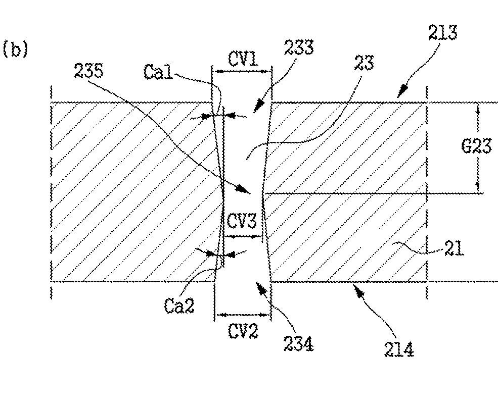
Why this shape matters is that drilling the hole is not the end — it has to be filled with copper. Taking the worked example in the Absolics patent, glass 300μm thick has a waist diameter of 75μm, an aspect ratio of 4 to 1, and the waist sits at 40 to 60% of the thickness from the entrance, 45 to 55% in the worked example. The very middle, narrowed from both sides, has to be filled without voids. Glass is an insulator, so plating requires laying down a thin copper seed layer first, and metal does not adhere well to bare glass. So an adhesion layer of a metal such as titanium or chromium, or a metal oxide such as zinc oxide or titanium oxide, is laid down thinner than 100nm. On top of that an electroless plated seed layer is formed and the hole is filled by electrolytic copper plating.
Electrical behaviour changes with how completely it is filled. At 30GHz the insertion loss made by a single TGV is 0.48dB when only the wall is plated, 0.34dB when partially filled, and 0.23dB when fully filled. The more it is filled, the lower the loss. And filling a high-aspect-ratio hole without voids is exactly where things are stuck right now.
What does not carry over: glass breaks in a different way
That is what display handed over. The problem is what comes next.
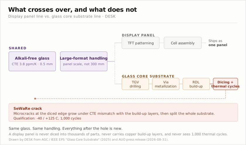
A display panel is a sheet of glass that becomes the product as it is. A glass core substrate is cut into thousands of pieces. And before it is cut, several layers of copper wiring are stacked on it. Those two things create failure modes display glass never meets.
It has a name. SeWaRe. Koizumi coined it in 2013 from the Japanese word for wood splitting. Microcracks left on the diced edge grow under the stress created by the difference in thermal expansion between the glass and the build-up layers stacked on it, and split the whole substrate horizontally.
A package substrate has to pass 1,000 cycles between minus 40 degrees and plus 125 degrees in this state. It is a condition a display panel has never once faced.
Changing the material does not solve it
The first answer that comes to mind for glass breaking is to use harder glass. But that answer does not work.
The theoretical strength of glass is very high. A silica fibre free of defects gives 10 to 15GPa at liquid nitrogen temperature and 5 to 6GPa at room temperature. Yet the strength of glass in actual use is about 100 times lower than that. Microcracks on the surface are the reason. Stress concentrates at the sharp tip of a crack, and from there the crack grows until it finally breaks.
Griffith’s fracture mechanics writes this in one line: critical stress is proportional to fracture toughness divided by the square root of crack size. Here things separate. Fracture toughness differs by only about ±10% among ordinary glass materials. Crack size, by contrast, varies several fold with dicing conditions, and on top of that it enters under a square root.
Change the glass and the curve barely moves. Raising fracture toughness from 0.68 to 0.82 lifts strength by only about 20%. Grow the crack 10 fold, on the other hand, and strength falls 68%. What can be gained by choosing a material and what can be lost by managing flaws are different in size.
So the actual countermeasures came from process and structure, not material. The dielectric and copper wiring of the build-up layers are made thin, blade dicing conditions are optimised, adhesion between the build-up layers and the glass is raised, and a pullback structure is applied that sets the build-up layers in from the substrate edge. Samples made this way showed no cracking or delamination after moisture absorption and reflow followed by 1,000 thermal cycles from minus 40 to plus 125 degrees.
The patent Absolics has been granted looks at the same place. What the claims set is not the type of glass but the deviation in residual stress. Within the same substrate, stress is measured on lines that pass through vias and lines that do not, and the difference is held to 1.5MPa or less, to 2.5MPa or less on lines with vias and 1.0MPa or less on lines without. It is a claim built on the premise that drilling a hole leaves stress around it and that the deviation becomes the origin of fracture. Instead of looking for harder glass, it went toward making the stress uniform.
Having a solution and getting that result every time under volume production conditions are different stories. That gap is showing up now in the schedules.
A 40% yield means one via fails 3.6 times in 100,000
How much precision the industry’s 40% yield actually demands can only be judged by knowing how many holes are drilled in one substrate. The Absolics patent seen earlier records that figure: 100 to 3,000 core vias per 1cm × 1cm unit area, and 225 and 1,024 in the worked examples.
Multiply that density by a 650mm × 550mm panel and the scale appears. At 1,024 per cm², that is 3.66 million on one panel. Narrow it to a 50mm × 50mm package big enough to carry one AI accelerator and it is still 25,600.
From here the arithmetic turns cruel. If the plating breaks or a crack forms in even one via, that package dies. Treating via defects as independent, package yield is the success rate of a single via raised to the power of the number of vias. Not addition but an exponent.
Working backwards gives this. For a package with 25,600 vias to reach 40% yield, the defect rate of a single via has to be 35.8ppm. That is 3.6 in 100,000. Which is to say the 40% the industry now calls “too low” already means succeeding at a single via with a probability of 99.9964%.
And to rise to the 60 to 70% vice president Gary Huang spoke of, this defect rate has to be cut 2.57 fold, from 35.8ppm to 13.9ppm. That multiple stays the same regardless of via count. For a package with 5,625 vias it is 162.9ppm to 63.4ppm, again 2.57 fold. Saying yield goes from 40% to 70% means cutting a defect rate already at 3 in 100,000 to below a third of that.
Here lies the structural trap of this technology. Glass was chosen for large area, and the wider the area the more vias there are and the more yield falls exponentially. At the same 35.8ppm, a small package with 1,000 vias gives 96.5%, one with 25,600 gives 40%, and one with 50,000 gives 16.7%. The area grown to push out silicon interposers cuts yield directly. Strength and weakness come from the same root.
This also explains why glass core substrates have reached a producible level while glass interposers slip past 2030. An interposer goes directly under the GPU and HBM, so wiring density is far higher and vias are denser in the same area. The number riding on the shoulder of the exponent grows. At the same process maturity the result is entirely different.
Why the Absolics patent claimed stress uniformity of all things also reads out here. Reducing the deviation of each individual via is the work of pushing the base of the exponent up toward 1, and in a place raised to the ten-thousandth power that small difference decides everything.
By the patents, the owner is not display
One thing has to be pointed out here. It is true that what display built over 30 years is carrying over, but that does not mean the display industry becomes the owner of this market.
Material analysing the patent landscape of glass core substrates and interposers shows Intel currently holding nearly half of the patents. The closest competitor is SK affiliate Absolics, and the remaining 70 or so companies each hold small numbers. Before 2020 there was no clear patent leader, and filings began rising around 2015.
There is no panel company near the top of that list. As the Absolics patent seen earlier shows, the core claims of a glass core substrate hang on via cross-section geometry, stress, and wiring structure. What display hands over is not patents but hands — the manufacturing ability to move large-area glass without breaking it and to lay fine wiring uniformly on top.
AUO’s position shows exactly that. AUO’s RDL process on Corning’s glass, shown in Corning’s booth.
All three companies pushed their schedules back
The phrase “world’s first volume production within the year” has been repeated for several years around this technology. Lay the actual schedule out in order and it reads differently.
Absolics, a joint venture of SKC and Applied Materials, completed a dedicated glass substrate plant in Georgia in the United States in 2024. Volume production moved from late 2025 or early 2026, to certification completed in 2026, and now to volume production in 2027. The reason pointed to is that the range of reliability testing required has widened because customers’ operating environments differ, from data centres to AI accelerators.
Samsung Electro-Mechanics slipped more recently. According to a report on 12 August, a target of operation in the second half of 2027 moved to 2028 or later, and the cause is failure to pass reliability evaluation of prototypes by a global communications semiconductor customer. Equipment orders have also been pushed back three or more times from a schedule of November 2025. The joint venture Glassem was set up by Samsung Electro-Mechanics and Dongwoo Fine-Chem, and the production line goes into Dongwoo Fine-Chem’s Pyeongtaek site. Dongwoo Fine-Chem is a Korean subsidiary wholly owned by Sumitomo Chemical, a display materials company that has made polarising film and touch sensors for LCD and OLED.
LG Innotek moved its commercialisation point from 2028 to 2030.
The reason all three slipped in the same direction is yield. By the Yole Group tally, current glass interposer yield is around 40%. Vice president Gary Huang called that figure too low, saying cost efficiency will be hard to secure unless it rises to 60 to 70%.
Two things were named as bottlenecks: the plating that carries signals through the glass, and the microcracks tied directly to substrate durability. Exactly the two the IEEE document pointed to earlier. Items the academic literature wrote down as tasks are pushing schedules back on the industrial floor.
There is one more thing to separate. What the press bundles together as “glass substrate” is really two things. A glass core substrate changes only the skeleton of the package substrate to glass; difficulty is relatively lower and it has reached a producible level. A glass interposer changes the wiring layer itself, directly under the GPU and HBM, to glass; difficulty is far higher and full commercialisation is seen past 2030. The 40% yield above is a figure for the interposer side. Read the two mixed together and both schedule and difficulty come out wrong.
Outlook
The migration of display glass technology into semiconductors will not reverse. The reason glass was chosen is physics, not fashion. Silicon is locked in a 300mm round wafer and organic substrates lose flatness at large area. As long as chiplets keep growing, the only material that gives large area, low loss and low warpage at once is glass, and the experience of handling that glass by the panel is only in display.
The commercial initiative in this technology, though, will not come to the panel companies. The patents are already held on the semiconductor side, and the remaining bottlenecks, plating and cracking, are both problems that did not exist in panel processes. Panel companies are likely to stand in the position of taking on process work between the materials firms and the semiconductor firms. The shape of AUO standing in Corning’s booth is the preview.
The timing looks like 2027 to 2028. And that is for glass core substrates only. The road from 40% to 70% is the work of cutting the defect rate 2.57 fold as calculated above, taking a value already at 3 in 100,000 down to a third again. It is not the kind of thing fixed by one plating change; dicing and stress management have to come up together, so it takes years. Glass interposers have denser vias and a bigger shoulder on the exponent, so they are unlikely to reach the market before 2030.
Whether this forecast was right or wrong can be seen from four things. First, whether Absolics announces that it has passed customer reliability certification. Quality testing is under way with AMD, Amazon and Intel, so if that announcement comes, 2027 volume production becomes a real schedule. Second, whether a yield above 60% is confirmed. It is the break-even line Yole Group put forward, and before that is crossed, whatever any company announces is trial production. Third, whether Samsung Electro-Mechanics’ equipment orders are actually placed. Having been pushed back three times, it is the most honest indicator. Fourth, whether announcements and articles begin distinguishing glass core substrates from glass interposers. Adding one more to that: whether the yield being announced states what area it is based on. Yield changes exponentially with package area, so a yield quoted without an area is a number that cannot be compared.
The fourth will be answered soonest. And it becomes the scale for reading the other three. Announcements that mix the two are usually covering the difficulty of the interposer with progress on the core substrate. If a company starts writing them separately, that company is likely to be genuinely ahead.