
Why IGZO, a display backplane material, went to memory
IGZO has been used for more than 20 years as nothing but the switch behind the screen. A Dongguk University group stood it up as the resistive switching layer of a vertical memory. The key was ALD rather than sputtering, and the switching only came alive once the In:Ga:Zn ratio was pushed toward gallium, as far as 1:3:1. It shows how far a material display process teams already know can be extended.
DOI 10.1002/advs.77076IGZO is the oxide semiconductor the display industry has handled longest and most. It has been used for more than 20 years as the channel of the thin-film transistor (TFT) that turns pixels on and off behind the screen, and its high mobility and large-area uniformity are properties already proven. Yet studies using this material not as a transistor but as the resistive switching layer of a memory are surprisingly few. The paper points at this directly. Most IGZO research has crowded into planar oxide semiconductors for displays, and studies digging into it as the active switching layer of an RRAM have remained a minority.
The Dongguk University group filled that blank in a 3D vertical structure. They opened a hole, coated its sidewall with IGZO 5 nanometers thick to make a device that changes the resistance between top and bottom electrodes, and designed a single device to hold both a state that remembers briefly and a state that remembers for a long time.
1. Why it was a hard problem
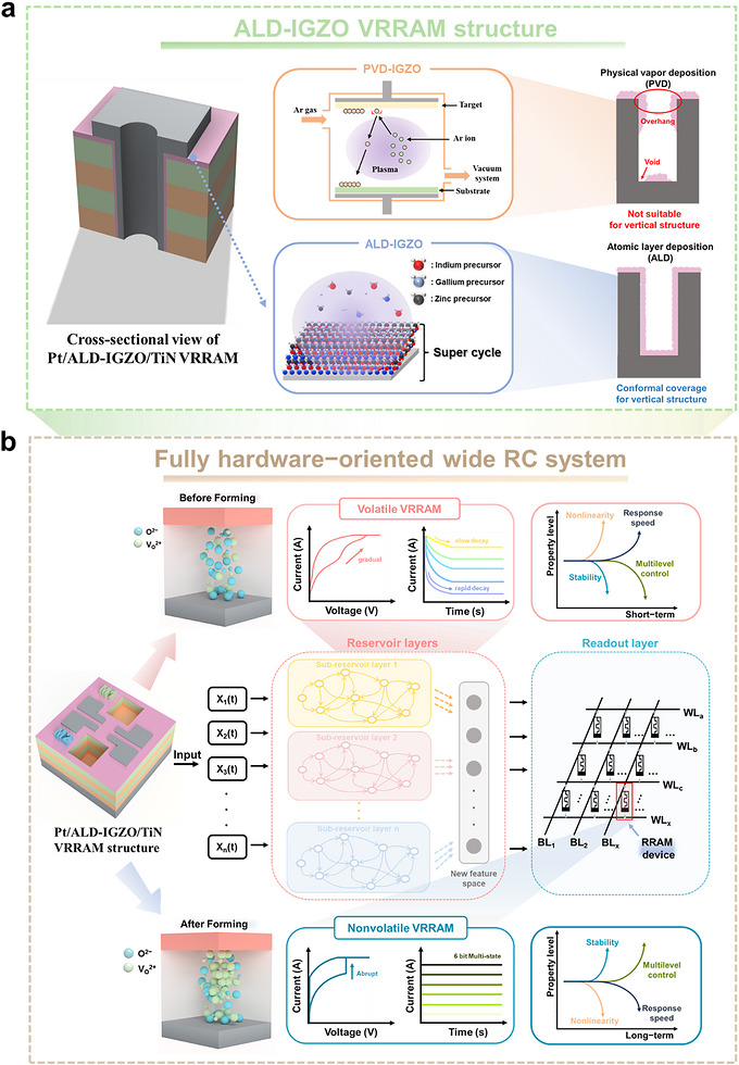
Handling a material in a vertical structure is completely different from a plane. The sidewall of a hole sits at a different angle from the floor, so scattering atoms from above does not coat the side evenly.
The method display production lines use to lay down IGZO is exactly that “scattering from above,” physical vapor deposition (PVD, sputtering). On a flat glass substrate there is no problem, but inside a vertical hole the sidewall coverage thins and breaks. The paper notes that studies leaning on sputtered IGZO were in fact held back by poor step coverage and erratic switching characteristics.
2. What they did and how
The method the group chose is plasma-enhanced atomic layer deposition (PEALD). Because it builds up one atomic layer at a time, it attaches to the sidewall of a hole at the same thickness. The process conditions are 150 degrees and 10 millitorr. The reason for plasma rather than thermal ALD is also clear. This is work laying another film over a structure already stacked layer by layer, so it must not thermally damage the layers below.
Here comes the part most interesting to a display engineer. Unless the composition was pushed heavily toward gallium, the device did not work at all.
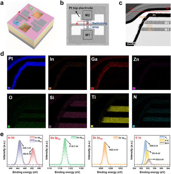
The group set the subcycle counts of indium, gallium and zinc oxide at 3 to 9 to 1 to reach a final composition of 1 to 3 to 1. The growth per cycle of each oxide was different. Indium grows 0.08 nanometers, gallium 0.10 nanometers and zinc 0.25 nanometers in one cycle.
Distinct resistive switching appeared only in this gallium-rich composition (1:3:1); in compositions with less gallium, current flowed like a metal with no resistance change. The reason is oxygen vacancies. With less gallium the metal-oxygen bond is weaker, so oxygen vacancies form in excess, free electrons become too many, and an off state is never created in the first place. Raising gallium hardens the bonding network, suppressing the spontaneous formation of oxygen vacancies, and only then can voltage move those vacancies to turn the device on and off.
The finished film was very flat, with an average surface roughness of 0.144 nanometers, and cross-sectional transmission electron microscopy confirmed that it covered the sidewall of a 10 micrometer diameter contact hole uniformly at 5 nanometers thick. The device structure stacks platinum, IGZO and titanium nitride, with the two titanium nitride electrode layers separated by silicon oxide into 2 tiers.
3. One device remembers in two ways
The core of this work is in dividing one device into two modes of use.
Before forming, a state does not hold long even when current flows. Apply 4.5 volts and the current rises, crossing from high resistance to low resistance, and it returns at minus 5 volts. But leave it in the on state and the current falls away quickly. It is a property that forgets with time. It looks like a defect at first glance, but in reservoir computing, which processes signals arriving over time, this “forgetting” is exactly the function required.
After forming, the opposite: the state stays. It serves as the readout layer holding learned weights.
The reliability figures for the two modes are as follows.
| Item | Condition | Result |
|---|---|---|
| Volatile switching endurance | 2V pulses repeated | 50,000 cycles, on/off resistance ratio held around 10 |
| Conductance modulation range | average over 100 cycles | 0.222µS, no systematic decline |
| Nonvolatile switching endurance | read voltage -0.1V | 5,000 cycles |
| Data retention | read voltage -0.1V | 10,000 seconds |
| Analog weight tuning | set 3V, reset -2V, 0.05 seconds each | smooth rise and fall over 50 consecutive pulses |
Behavior resembling a biological synapse was confirmed as well. Measuring while widening the interval between two pulses from 0.1 seconds to 3 seconds, paired-pulse facilitation appeared exponentially, with the second response larger the shorter the gap. The “rate of forgetting” itself also changed with the applied voltage. At minus 1 volt the current disappeared quickly, but at plus 1 volt the state held for 40 seconds. It means different time constants can be made with the same device.
4. Results
The group implemented in hardware a configuration that widens the reservoir by placing several devices with different volatility side by side (wide RC), and applied it to classifying handwritten digits and clothing images.
| Task | Wide reservoir | Single reservoir |
|---|---|---|
| MNIST handwritten digits | 91.31% | 84.39% |
| Fashion-MNIST clothing | 82.73% | 79.9% |
The energy for one classification was estimated at 3.70 nanojoules. Because both reservoir and readout are handled by devices in a fully hardware configuration, the structure is simpler than approaches that left readout to software.
5. What it means
From the display industry’s side, the value of this paper lies less in the performance figures than in the extensibility of the material and the process.
First, the use of IGZO goes beyond the switch behind the screen. If a material in which panel makers and material makers have already accumulated 20 years of know-how takes a place as the active layer of a 3D memory, that know-how becomes worth something as it stands.
Second, ALD moves firmly onto the list of options for IGZO processing. The point at which this work states that sputtering would not do and only ALD would was sidewall coverage in a vertical structure. Displays meet the same problem as pixels shrink and structures go three-dimensional. The moment the ability to coat a sidewall uniformly is needed, the PEALD conditions and composition design this paper sets out become reference material as they are.
Third, the lesson in composition design is clear. Even with the same IGZO, where you put the ratio of indium to gallium makes the device an entirely different object. In a TFT, indium is raised for mobility, but in this device gallium had to be raised three times over to suppress oxygen vacancies before an off state was created at all. For anyone working with oxide semiconductors it is a contrast that is familiar and still worth confirming again.