Radical OLEDs Where Charge Balance Sets Both Efficiency and Roll-off
Researchers at Yonsei University and the University of Cambridge built a near-infrared OLED from a radical emitter. Switching hosts dropped the film photoluminescence efficiency from 21% to 8%, yet device efficiency stayed almost the same at 6.2% and 5.7%. Charge balance made up for the photoluminescence loss. Securing both together delivered an EQE of 8.1%, and holes were identified as the culprit that cuts efficiency at high current.
DOI 10.1002/adfm.78903The efficiency ceiling of an OLED comes from spin. Of the excitons created by current, only one in four is a singlet and the other three are triplets, so fluorescent materials stop at 25%.
Until now there have been two ways past that ceiling. Phosphorescence uses heavy metals to turn triplets into light, and TADF lifts triplets back up to singlets. Both were questions of how to deal with triplets.
Radical emitters sidestep the question itself. They are open-shell molecules with an unpaired electron, so the ground state is a doublet and so is the excited state. There is no spin-forbidden transition to begin with, so there are no triplets to manage.
The device this paper covers is a near-infrared OLED made from such a radical. Its wavelength is 804 nanometers, not a display color. This section still picked it because the finding is not tied to the wavelength.
While building devices with different hosts, the researchers ran into a result they could not explain. The film photoluminescence efficiency fell to one third, yet device efficiency stayed almost the same.
Digging into that gap produced two conclusions. Charge balance and emission efficiency cannot be chosen separately, and the same charges are also the culprit that cuts efficiency at high current.
1. Why do radical emitters sidestep spin statistics?
Because they are open-shell molecules with an unpaired electron from the ground state up, so the emissive transition takes place between doublets. An ordinary molecule with only paired electrons has a singlet ground state, and three quarters of the excitons created by current become triplets that cannot be used for fluorescence.
In a radical, one electron is left unpaired. Both the ground state and the lowest excited state of the molecule are doublets, and the transition between them is spin-allowed. The task of harvesting triplets never arises.
In a real device, though, that is not the end of it. The device in this paper mixes the radical emitter TPA-PyBTM′ into a host at only 3%. Most excitons created by current form on the host, and they must transfer to the radical to become doublet emission.
That transfer is the battleground of this piece. Depending on the host, how evenly charges come in and how much energy is lost on the way over both change together.
2. Why was device efficiency the same when photoluminescence efficiency was one third?
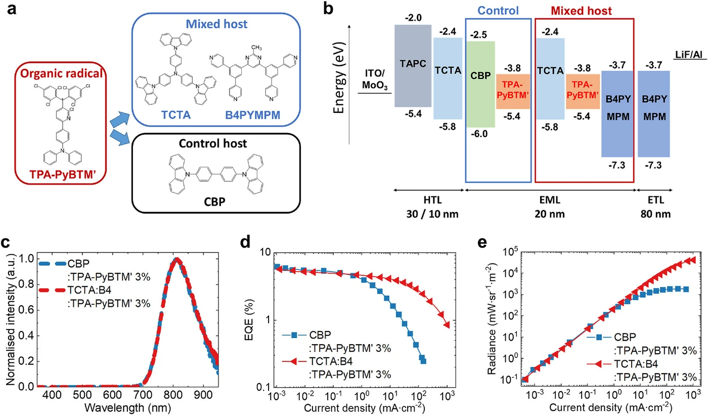
Because charge balance almost made up for the photoluminescence loss. A film with the radical in the wide-gap host CBP has a photoluminescence quantum efficiency (PLQE) of 21%, and a film in the exciplex host (TCTA:B4PYMPM) has 8%. That is nearly three times lower.
Yet as devices, the peak external quantum efficiencies are 6.2% and 5.7%. Almost the same. The threefold gap in the films disappeared in the devices.
The exciplex host earned it back on the charge side. The exciplex formed by the two transport materials removes the injection barrier and lets electrons and holes in evenly. With balanced recombination, the same current creates more excitons.
It loses on the energy side instead. The excitation pathway through the exciplex creates a large energy loss along the way, and that shows up as the 8% film photoluminescence efficiency. What was earned and what was lost cancelled out, leaving device efficiency where it was.
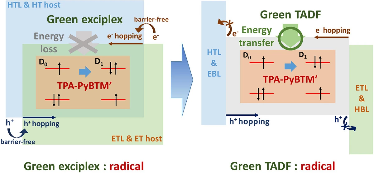
This observation overturns a design guideline. If film photoluminescence efficiency is used as the metric for evaluating radical emitters, it does not tell you what will happen in the device. How charges come in carries equal weight.
3. The green TADF host that reconciled the two
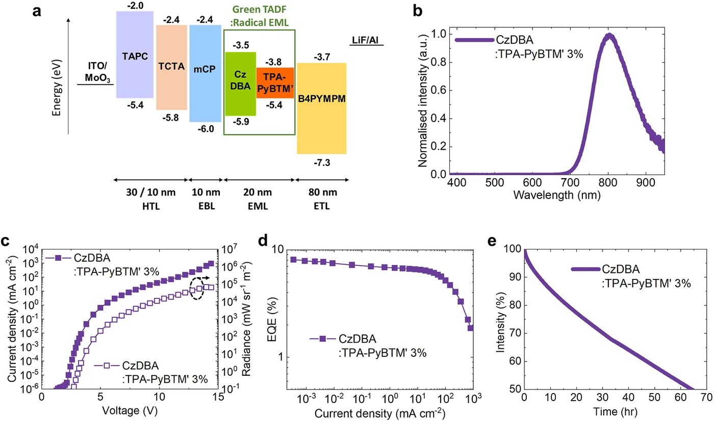
If it is a matter of earning and losing, the answer is to find a host that secures both. The researchers chose the green TADF material CzDBA. Its neat film has a photoluminescence efficiency above 90%, and it is bipolar, carrying both electrons and holes.
The overlap fit as well. The radical emitter’s absorption spreads broadly from the ultraviolet to the green, so it overlaps well with CzDBA’s emission, and energy transfer is efficient. This film’s photoluminescence efficiency is 26%, clearly higher than the exciplex systems (below 10%).
The path the energy takes also differs from ordinary hyperfluorescence. In transient photoluminescence, adding the radical makes the onset of delayed emission earlier than in pristine CzDBA. If delayed FRET dominated, the onset should resemble the pristine film, so this result points to intersystem crossing followed by Dexter energy transfer (DET) as the main pathway. FRET and DET both contribute.
Device performance rose accordingly: an external quantum efficiency of 8.1% (804 nanometers) and a maximum radiance of 70,800 mW/sr/m². Compared with the exciplex reference device, efficiency is more than 40% higher and radiance more than 70% higher.
| Host | Film PL efficiency | Peak EQE | Note |
|---|---|---|---|
| CBP (wide-gap) | 21% | 6.2% | Good photoluminescence, unfavorable charge balance |
| TCTA:B4PYMPM (exciplex) | 8% | 5.7% | Good charge balance, loses on energy |
| CzDBA (green TADF) | 26% | 8.1% | Bipolar + high photoluminescence efficiency |
Roll-off was suppressed too. More than 80% of peak efficiency remains at 10 mA/cm², and even at 100 mA/cm² it holds 5.2%, over 60% of the peak. The turn-on voltage is 2.7 V, and the lifetime at 0.1 mA/cm² is about 65 h, 35% longer than the exciplex device.
4. What cuts efficiency at high current?
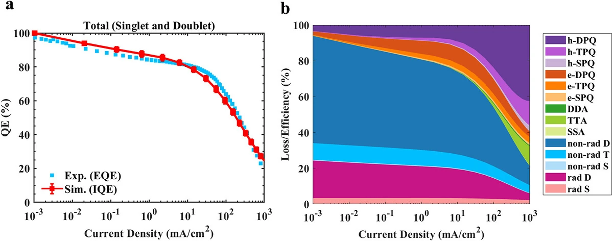
Holes. The researchers solved the coupled Poisson and drift-diffusion equations to compute the charge and exciton distributions inside the emitting layer, then split the loss pathways by type and tracked them against current density.
At low current, nonradiative decay within the doublet channel itself limits efficiency. Hole-induced and electron-induced quenching follow as secondary pathways.
At high current the landscape changes. Hole-induced doublet-polaron quenching (h-DPQ) becomes the dominant loss in the doublet channel. The more efficient hole injection is, the faster the hole density in the emitting layer rises, and those holes quench doublet excitons. The electron side (e-DPQ) contributes noticeably in the intermediate current range (10 to 100 mA/cm²).
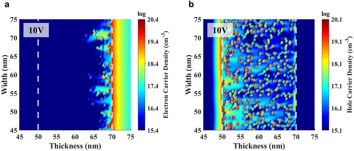
In the same current range, triplet-polaron quenching (h-TPQ) and triplet-triplet annihilation (TTA) rise as well. This means that under high injection, both polaron-exciton interactions and exciton-exciton annihilation grow.
In the internal quantum efficiency curve, that transition appears as a threshold around 76.8 mA/cm² (9 V). Below and above it, the owner of the loss is different.
Magnetic field measurements provide supporting evidence. At low current (10 mA/cm² or below), a positive magneto-electroluminescence response appears, a sign that triplet-to-doublet Dexter transfer is at work, consistent with the delayed component in transient photoluminescence.
This section is where the paper is worth the most. It does not stop at describing roll-off as “efficiency drops at high current”; it separates which quenching owns which current. What to reduce next comes out of that breakdown.
5. Between the abstract and the body
The abstract says charge balance and emission efficiency were secured together. Go into the body and four conditions attach.
First, 804 nanometers is invisible light. This device is not for displays; its applications lie in biosensing, optical communication, and night-vision lighting. The finding reaching OLEDs in general and this device being used in displays are different stories.
Second, the 8.1% efficiency is a number within the near-infrared. Against reported values in the 800 to 900 nanometer range it is a good value, but it should not be set beside the 20 to 30% range of visible phosphorescent and TADF OLEDs. Radical OLEDs are not there yet.
Third, the 65 h lifetime was measured at 0.1 mA/cm². That is a very low current, far from the conditions displays demand. “35% longer than the exciplex device” should be read as a relative comparison.
Fourth, the loss breakdown is a simulation result. The evidence is that the coupled Poisson and drift-diffusion calculation reproduced the shape of the measured external quantum efficiency curve; h-DPQ was not pinned down directly by spectroscopy. The magneto-electroluminescence measurement supports the Dexter transfer side, but naming the culprit among quenching pathways rests on the simulation.
And there is one thing we looked for but did not find: what happens when radical emitters are used with the same design in the visible. The paper’s conclusion is built on host bipolarity and energy overlap, so it looks as though it would hold when moved to the visible, but that check is outside its scope.
6. What’s left for industry
This device will not go into a panel any time soon. It is near-infrared, and both efficiency and lifetime fall well short of display standards.
This piece still treated it in depth because there are two things that can be carried over.
One is the place of the evaluation metric. It shows in numbers that the habit of ranking emitters by film photoluminescence efficiency does not work for radical systems. The evidence is the threefold film gap of 21% and 8% narrowing to 6.2% and 5.7% in devices. If the host’s charge transport properties carry equal weight, both must be measured together at the material screening stage.
The other is the method of splitting roll-off by culprit. If the owner differs by current range, so does the remedy. If nonradiative decay owns low current, the molecule must be fixed; if hole-induced quenching owns high current, injecting holes more efficiently becomes the problem rather than the answer. This reversal exists in the same form in roll-off discussions for phosphorescent and TADF devices.
The remaining question is clear: where is the ceiling of doublet emission? Whether the price of sidestepping spin statistics is greater vulnerability to polaron quenching, or whether this is a trait of this particular structure, the paper does not answer. A comparison becomes possible only once visible radical OLEDs arrive.