Gentler Corrugation Boosts Top-Emitting OLED Outcoupling
Researchers at Kyung Hee University made the internal light-extraction structure of a top-emitting microcavity OLED gentler. A more deeply etched microlens array sent only 43.5% of the light forward; a gentle corrugation sent 77.3%. Even with low roughness, a steep local slope unsettled the cavity. The result says that disturbing the cavity less comes before scattering harder.
DOI 10.1002/advs.78013A top-emitting OLED sends its light out away from the substrate. That decouples the aperture ratio from the backplane layout, which is why high-resolution panels use this structure.
A Fabry-Pérot microcavity comes along almost automatically. The top and bottom metals act as mirrors that favor specific wavelengths, so the emission spectrum narrows and the light gathers toward the front. Forward efficiency and color purity rise together.
That strength is also the constraint. Gathering light toward the front means color shifts with viewing angle, and because the cavity already dictates the spectrum, there is little room left to insert a light-extraction structure.
The trapped light is not a small share. An OLED stack harbors channels called waveguide modes and surface plasmons, and reworking only the air-side interface cannot recover that light. You have to reach inside.
The conventional wisdom for internal light extraction is corrugation: add wrinkles or stamp microlenses to scatter the trapped modes. But strong corrugation smears the angular distribution, scrambles the narrow spectrum the cavity created, and degrades the uniformity of the layers deposited on top.
Researchers at Kyung Hee University went the other way at this point. They made the corrugation gentler. And it beat the more deeply etched alternative.
1. The cavity narrows the room for light extraction
The cavity has already fixed the spectrum and the angles. In a flat cavity, the optical thickness between the top and bottom mirrors must be the same across the whole screen for a single resonance condition to hold. That condition is the basis for forward efficiency and color purity.
Putting corrugation inside means deliberately perturbing that optical thickness. Stack organic layers and electrodes on top of a corrugation, and the stack thickness differs between valleys and peaks, so the local resonance wavelength varies from spot to spot.
This is the geometric weak point the paper identifies. If the underlying surface is steep, the upper layers cannot cover it conformally, and the local optical thickness variation grows. Scattering gets stronger, but the gain the cavity provided is cut by the same amount, so nothing is left over at the device level.
So the design goal the researchers set was not to increase scattering. It was to extract trapped modes while preserving the local resonance, and as the condition satisfying both they defined a gentle internal corrugation layer (GICL) with “a low representative surface angle and broad lateral modulation.”
The cavity was set at second-order resonance. A thicker organic stack is less vulnerable to particle-induced leakage and deposition non-uniformity; the added thickness went mainly to the hole transport layer, keeping the electron transport layer thin and preserving the intended resonance.
2. Why does etching deeper let less light out?
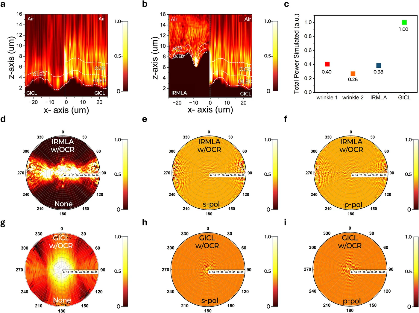
Because the light only spreads wide instead of coming forward. In FDTD simulations run under identical conditions, the gentle corrugation (GICL) sent 77.3% of the input power into the forward collection region, while the steep microlens array (IRMLA) sent only 43.5%.
Where the rest went is shown too. The wide-angle component is 11.4% for GICL but 43.6% for IRMLA. The strong corrugation did extract the light, but at angles that can’t be used.
Surface-geometry numbers explain the difference. Over a 50×50-micrometer scan area, GICL has a peak-to-valley height of 1,118 nanometers, an RMS roughness of 144.5 nanometers, and a representative surface angle of 2.1–6.9° along x and 1.8–3.5° along y. IRMLA has a roughness of 1,359 nanometers, a peak-to-valley height of 7,867 nanometers, and a representative surface angle of 25.3°.
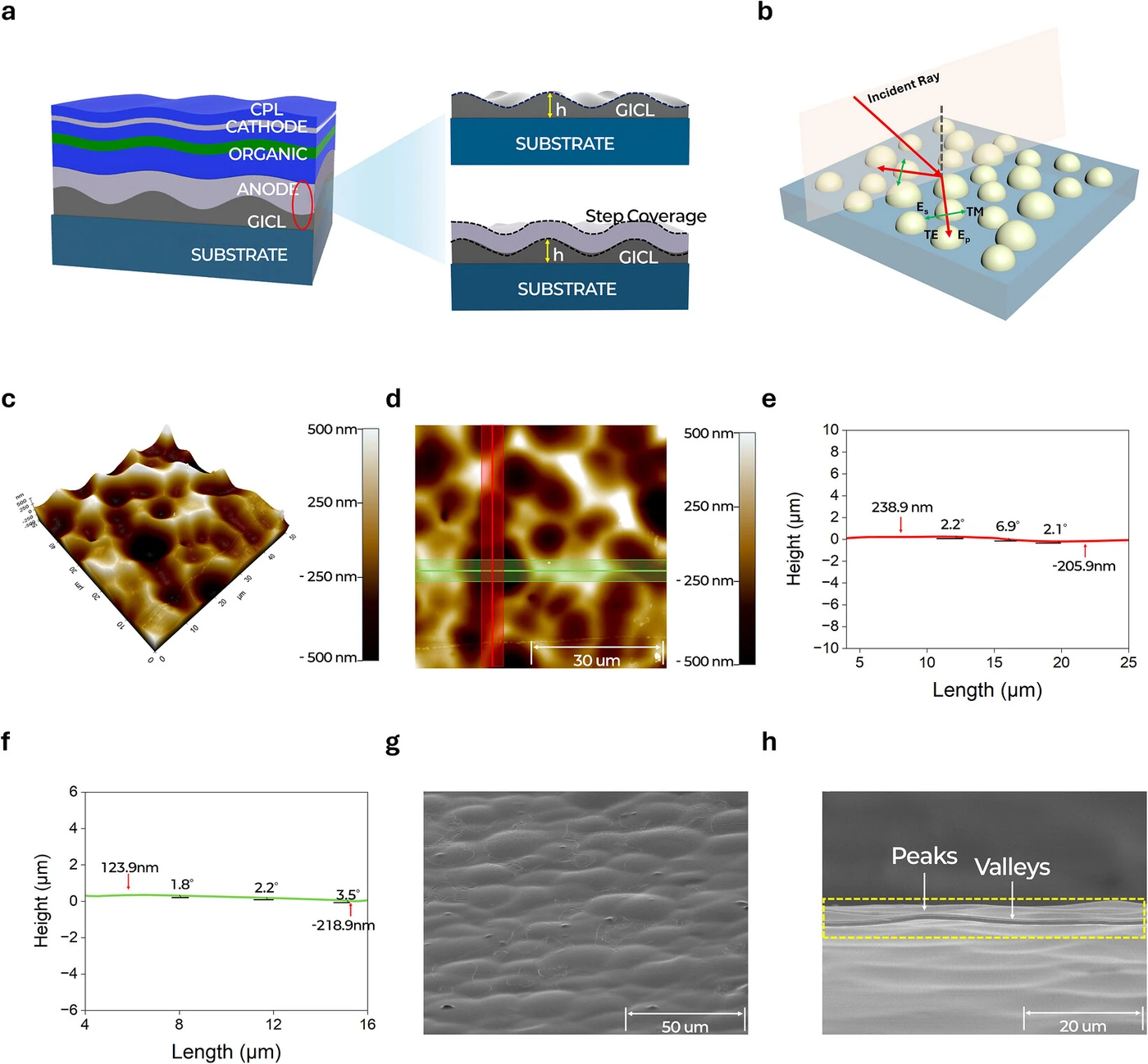
But the point this article wants to flag is not roughness — it is slope. The deep wrinkle in the comparison set (wrinkle 2) has a roughness of only 48.4 nanometers, yet representative surface angles of 55.7° and 53.1°. By roughness alone it is 1/3 of GICL, but its local geometry is far steeper.
The paper puts one sentence right there: low roughness amplitude does not imply gentle local geometry. The simulation results are summed up the same way: “simply strengthening the perturbation does not improve the optical response.”
| Structure | RMS roughness | Peak-to-valley height | Representative surface angle | Forward collection | Wide-angle component |
|---|---|---|---|---|---|
| Shallow wrinkle (wrinkle 1) | 20.6nm | · | 1.5° · 2.2° | · | · |
| Deep wrinkle (wrinkle 2) | 48.4nm | · | 55.7° · 53.1° | · | · |
| Steep microlens array (IRMLA) | 1,359nm | 7,867nm | 25.3° | 43.5% | 43.6% |
| Gentle corrugation (GICL) | 144.5nm | 1,118nm | 2.1–6.9° | 77.3% | 11.4% |
Forward collection and wide-angle components are FDTD values computed at 532 nanometers under the same dipole conditions. In the same calculation, with optical resin and transparent electrode conditions matched exactly, light extraction efficiency (LEE) went from 37.6% for the flat device to 74.1% for the gentle-corrugation device — 1.97 times.
3. Where did the trapped light come back from?
It came back from waveguide modes; surface plasmons stayed almost untouched. Breaking optical power down by channel, the flat device (P-O2) splits into 29.7% extracted · 40.0% waveguide modes · 30.4% high-wavevector components associated with surface plasmons.
In the device with the gentle corrugation (G-O2), extraction rose to 38.6% and waveguide modes fell to 32.0%. The surface-plasmon-related component moved by only 1 percentage point, from 30.4% to 29.4%.
This means light bound close to the metal is hard to extract with corrugation. Surface plasmons are tightly tied to the electrode interface, beyond the reach of micrometer-scale geometry, and they remain an open problem for top-emitting structures.
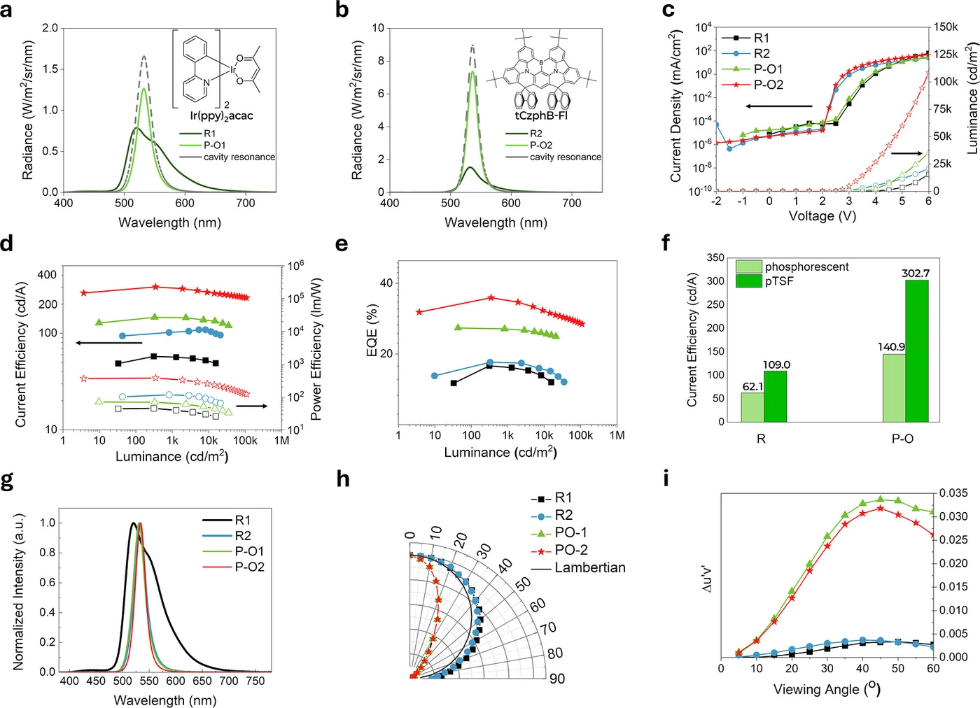
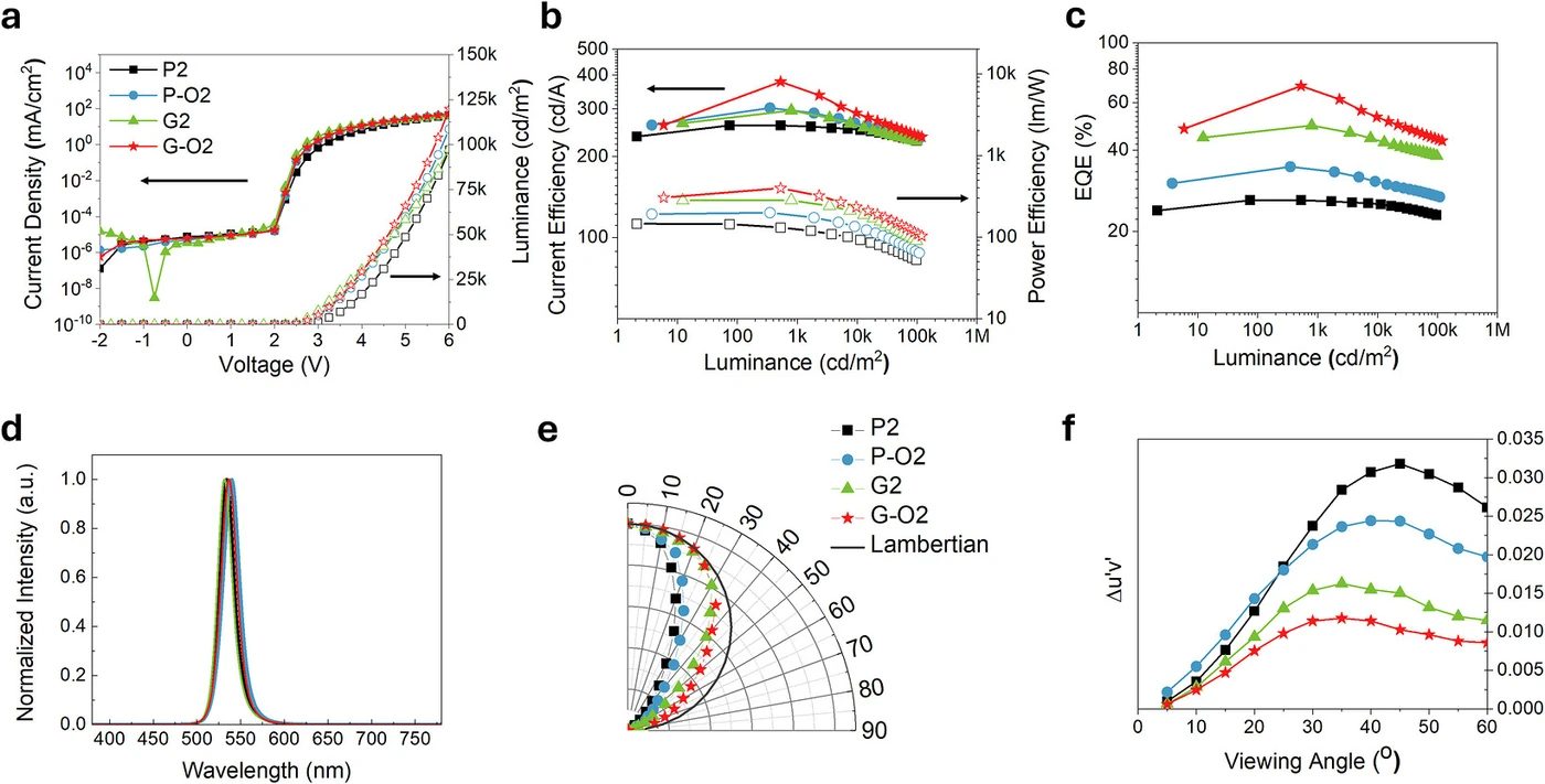
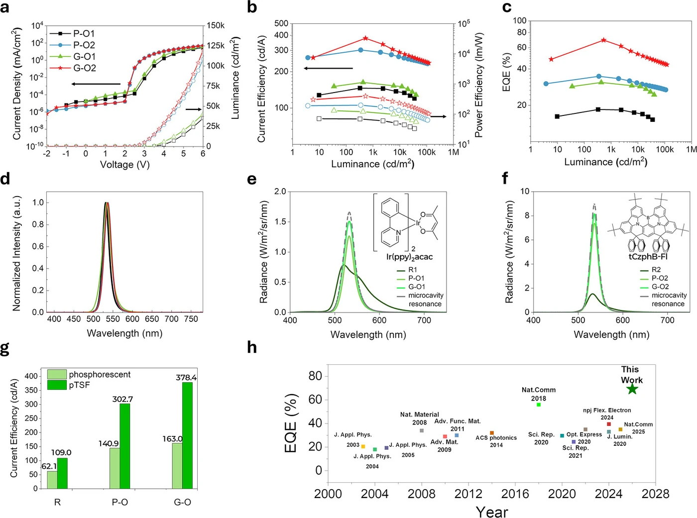
The device numbers point the same way. Under the condition with identical optical clear resin (OCR) applied, forward current efficiency rose 25.0%, from 302.7 cd/A to 378.4 cd/A.
Metrics that go through Lambertian correction move further. After correction, power efficiency rose from 199.3 lm/W to 396.7 lm/W and external quantum efficiency from 34.8% to 69.2%, and the average peak external quantum efficiency across five samples was 34.2±0.6% versus 68.2±0.7%. Pre-correction and post-correction figures are numbers on different bases.
4. Why the same corrugation works differently by emitter
The gain was larger with the narrower emitter. With the same gentle corrugation, the phosphorescent system’s current efficiency rose from 140.9 cd/A to 163.0 cd/A — 22.1 cd/A (15.7%) — while the pTSF system’s rose from 302.7 cd/A to 378.4 cd/A — 75.7 cd/A (25.0%).
The paper points to emission linewidth as the reason. The phosphorescent system’s emission FWHM is 25 nanometers even after the cavity, and the pTSF system’s is 19 nanometers. Narrower means a larger share stays inside the cavity resonance band.
The pTSF system has a TADF host (DMIC-TRZ) and a phosphorescent assistant (Ir(ppy)₂acac) jointly sensitizing a terminal MR-TADF emitter (tCzphB-Fl). It is a combination meant to use excitons efficiently while obtaining narrow emission.
But the authors draw a line themselves right there. Because the two emitter systems differ not only in FWHM but also in emitting-layer composition and electrical and photophysical properties, they write that the difference in gain cannot be attributed to FWHM alone. FWHM goes only as far as “an important spectral factor.”
5. Between the abstract and the body
There are four conditions to attach before copying the abstract’s side-by-side numbers into an internal report.
First, doubled external quantum efficiency is not doubled forward efficiency. A table footnote states that external quantum efficiency and power efficiency are values after applying a Lambertian correction factor (LCF), and that factor rose from 0.5238 for the flat device to 0.8343 for the corrugated device. Forward current efficiency, which receives no correction, rose 25.0%.
Second, the rise in that factor means the light spread out. A correction factor approaching 1 means the angular distribution is approaching Lambertian, and one of the values of a top-emitting microcavity is forward concentration. Total hemispherical light output rose at the cost of weaker forward concentration. The forward color coordinate also moved, from (0.2008, 0.7473) to (0.2271, 0.7459).
Third, angular color shift and forward color purity are separate stories. Peak shift out to 60° shrank from 13 nanometers to 3 nanometers, and angular color shift fell to Δu′v′ 0.0086. Angular variation clearly improved; the forward color coordinate shift noted above is a separate item.
Fourth, roll-off got worse. Relative external quantum efficiency roll-off at 10³ cd/m² is 0.5% for the phosphorescent flat device, 1.9% for the phosphorescent corrugated device, 2.7% for the pTSF flat device, and 4.6% for the pTSF corrugated device. The order in which efficiency rose matches the order in which roll-off worsened.
And there is one thing we looked for but did not find: lifetime data. How the process of embedding corrugation internally and stacking organic layers on it affects lifetime is outside this paper’s scope. The first item asked in any mass-production decision on a light-extraction structure is blank.
| Device | Current efficiency | Power efficiency | External quantum efficiency | Correction factor | FWHM | Peak luminance | Forward color coordinate |
|---|---|---|---|---|---|---|---|
| Flat (P2) | 260.7cd/A | 145.8lm/W | 26.1% | 0.4407 | 19nm | 97,174cd/m² | (0.1987, 0.7634) |
| Flat+resin (P-O2) | 302.7cd/A | 199.3lm/W | 34.8% | 0.5238 | 19nm | 108,659cd/m² | (0.2008, 0.7473) |
| Corrugated (G2) | 296.1cd/A | 281.9lm/W | 49.4% | 0.7576 | 21nm | 97,666cd/m² | (0.2305, 0.7417) |
| Corrugated+resin (G-O2) | 378.4cd/A | 396.7lm/W | 69.2% | 0.8343 | 22nm | 119,889cd/m² | (0.2271, 0.7459) |
Power efficiency and external quantum efficiency are values with the correction factor applied; current efficiency is not. They sit on the same row, but they are not numbers on the same basis.
6. What’s left for industry
What this paper changed is not the material but the decision criterion. Where internal light-extraction structures used to be ranked by roughness or depth, local slope and conformal deposition now enter as criteria.
There is one property the production side will welcome. A gentle corrugation is a shape that the layers stacked on it can easily cover. Because it reduces from the outset the step-coverage problems and local optical thickness fluctuations that steep structures cause, it places a relatively small burden on the deposition process.
On the other side, three things remain. There is no lifetime data, the nearly 30% share bound to surface plasmons is untouched, and the direction that raises efficiency overlaps with the direction that erodes forward concentration. If forward efficiency and color purity are why top emission was chosen, this trade-off has to be recalculated for each panel.
The scope of application carries conditions too. This result comes from a second-order-resonance green single-stack device. Blue and red differ in cavity thickness and resonance bandwidth, and stacked (tandem) devices have a different per-channel power distribution altogether. Nothing in this paper justifies assuming the same corrugation yields the same gain.