A Blue OLED That Reaches 1,000 cd/m² at 2.7 V
For most blue OLEDs, 2.7 V is barely the voltage at which light begins to show. A team at the Institute of Science Tokyo closed off the path by which triplets leak toward the anode, and got 1,000 cd/m² out of that same 2.7 V. The method is to gather low energy twice over to make blue. But the efficiency ceiling of this approach is 5.5%, and the device stands at 32% of it.
DOI 10.1002/adfm.78490Blue OLEDs have a voltage floor. A blue photon is worth about 2.7 electron volts, so to make an electron and a hole meet with that much energy generally costs somewhere around 3 V.
Gather up the recent blue OLEDs and it takes 3 to 6 V to reach 1,000 cd/m². For many devices, 2.7 V is the voltage at which light is only just becoming visible.
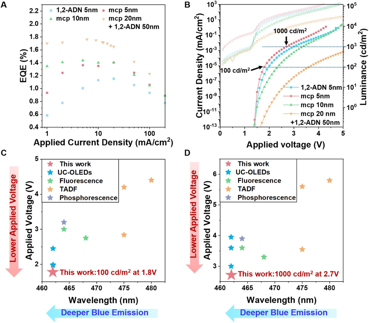
A team at the Institute of Science Tokyo got 1,000 cd/m² out of that same 2.7 V. 100 cd/m² came at 1.8 V. These are values that fit inside a single lithium-ion cell (3.7 V).
The trick is not to put the energy in all at once. Two low-energy states are made and then combined. This is upconversion, in which two triplets collide and produce a higher-energy emissive state.
What this paper did was close off the path by which those triplets leak toward the anode and vanish. Closing it brought the threshold current at which the device starts to light up down to 1/20.
And what this article wants to point to comes after that. The efficiency ceiling of this approach is 5.5%, and the device stands at 32% of it. A low voltage and a low power draw are not the same thing.
1. Why blue can be turned on at 2.7 V
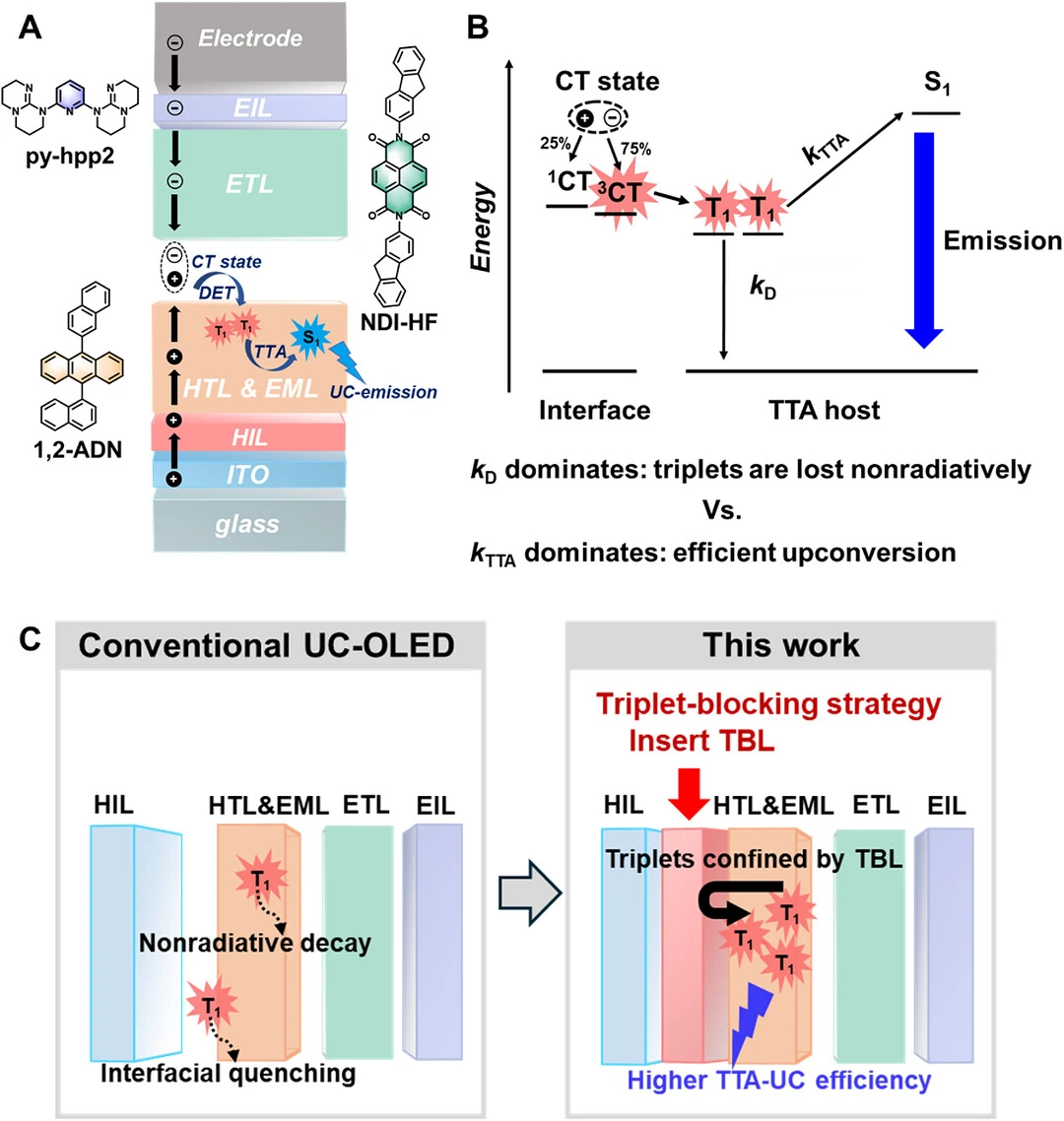
Because what the electricity makes is not blue. What charge injection directly creates in this device is a charge-transfer (CT) state at the face where two materials meet, and that state is lower in energy than a blue photon.
By spin statistics, 75% of those CT states are triplets. A triplet CT state passes by Dexter transfer into the triplet (T1) of the neighbouring material. Everything up to here belongs to the low-energy world.
Blue is made in the step after that. Two triplets meet, one of them becomes a high-energy singlet, and that singlet emits blue light. This is triplet-triplet annihilation upconversion (TTA-UC).
So this device emits blue at a voltage below the photon energy. The paper records that earlier work reported blue electroluminescence at 1.47 V.
2. So why did no efficiency appear at low current
Because it is a process in which two triplets have to meet, and if triplets are rare they never do. Upconversion is a second-order process in which two collide, while vanishing alone is first-order. When triplets are few, the first-order path wins.
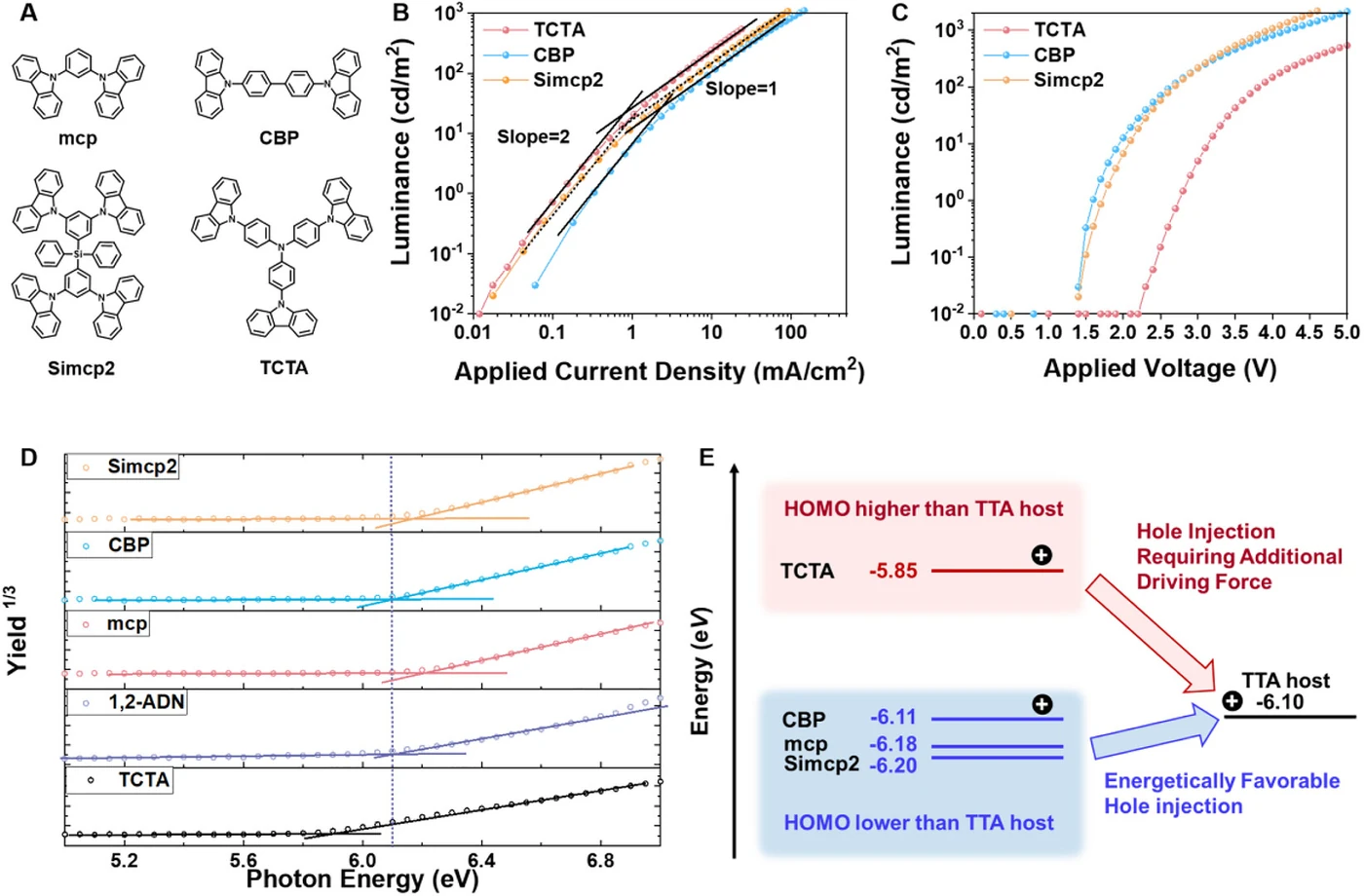
That is why an upconversion device has a threshold current density. Below it efficiency sits on the floor; only above it does efficiency take hold. Plot luminance against current on log axes and the slope bends from 2 to 1, and the bend is the threshold.
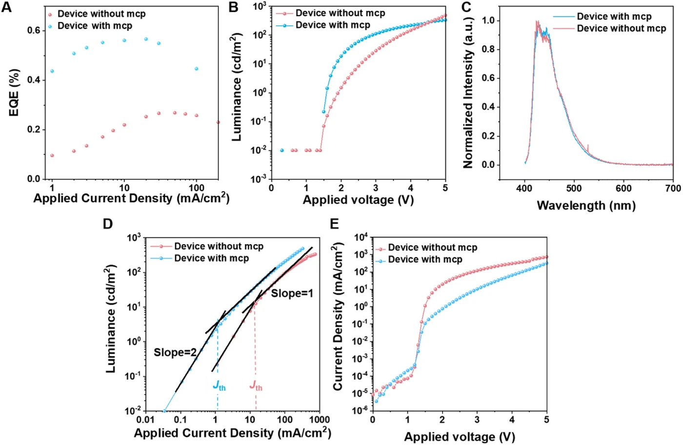
The reference device behaved that way. At 1 mA/cm² its external quantum efficiency stopped at 0.10%, and only on the way up to around 30 mA/cm² did it reach 0.27%. Producing 100 cd/m² took 3.7 V.
To run at low voltage you need efficiency at low current, and by the very principle of the thing that was the least favourable place.
3. Four checks on where the triplets were leaking
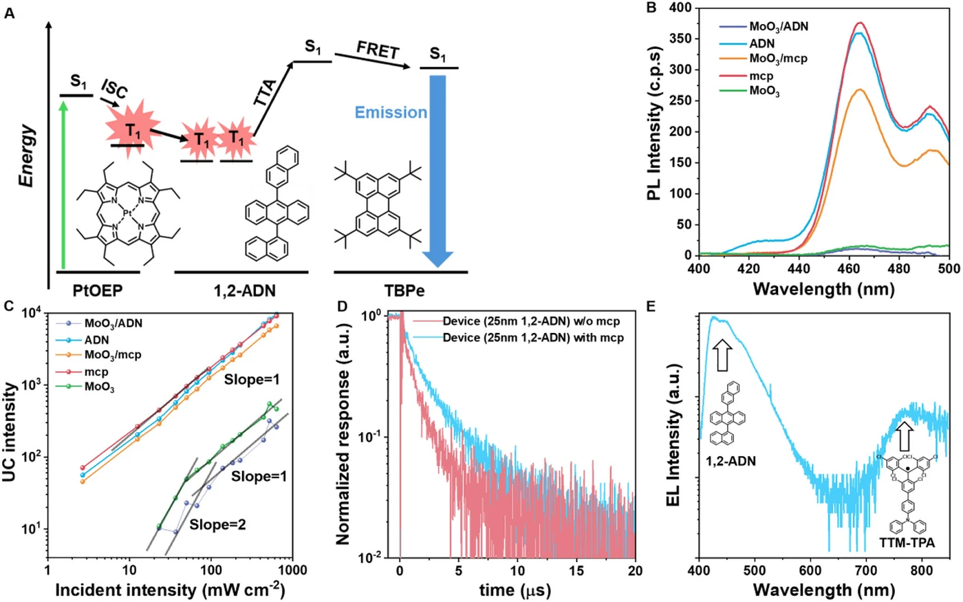
The molybdenum oxide (MoO3) interface on the anode side was the culprit. Before touching the device, the team confirmed it in optical experiments first.
They made a film in which platinum porphyrin generates triplets and upconversion takes place in the same host, and put MoO3 against it. The upconversion emission fell away by about 97%. Slipping an mcp layer in between brought the emission back to nearly its original level.
The device pointed the same way. Measuring the electroluminescence decay at 250 mA/cm², the delayed emission lived longer on the side with mcp. That means fewer triplets are being quenched.
They also built separate evidence that triplets really do walk all the way to the anode. A 5 nm layer doped with 3% of a radical emitter was buried right next to the anode, and that layer’s light came out together with the rest in the electroluminescence spectrum. Excitons born at the interface had travelled to the far side.
A thickness experiment backs this up. Thickening the host from 50 nm to 200 nm roughly doubled the efficiency. The further from the anode, the less quenching. But resistance rose and current would not flow at low voltage, so it was not practical.
4. One blocking layer cut the threshold current to 1/20
All it took was 10 nm of a material with a high triplet energy between the anode and the host. Triplets cannot cross into that layer, so they stay trapped inside the emitting layer.
The effect showed up at the threshold. The threshold current density came down from 20 mA/cm² to 1 mA/cm². The point where the luminance-current curve bends from slope 2 to slope 1 moved left by the same amount.
Efficiency rose along with it. The external quantum efficiency at 1 mA/cm², which had been 0.10%, climbed to the 0.4% range, and the peak value rose from 0.27% to the 0.5% range. The whole voltage-luminance curve was pushed to the left.
The price is resistance. With one more layer to cross, the current flowing at a given voltage dropped. This trade becomes the criterion that divides device designs later on.
5. With doping added, 100 cd/m² at 1.8 V and 1,000 cd/m² at 2.7 V
Emission was handed to a dopant rather than the host. Mix a blue fluorescent dopant (TBPe) into the host and the singlet made by upconversion moves onto the dopant and emits better. The emission peak is at 462 nm.
Comparing blocking layers of different thickness, the thicker the layer, the higher the efficiency and the lower the current. The device using a 20 nm blocking layer with a 50 nm host was the highest at 1.76% external quantum efficiency. That is 28.5% higher than the earlier report on the same material system (1.37%), and the paper records it as the best figure yet for a blue upconversion OLED.
But the most efficient device was not the most usable one. Its resistance is high, so brightness does not come at low voltage. The device with a 5 nm blocking layer and a 25 nm host struck the best balance.
That device produced 100 cd/m² at 1.8 V and 1,000 cd/m² at 2.7 V. Set against the recent blue OLEDs the paper collects, that is the lowest voltage at both brightness levels.
6. A high triplet energy turned out not to be the whole story
Four materials with amply high triplet energy were tried, and the threshold fell for every one of them, but the voltage differed for just one. mcp, CBP and Simcp2 lit blue at around 1.5 V, while TCTA had to go past 2.2 V before it lit.
The cause was not the triplet but the path by which holes go in. Photoelectron yield spectroscopy put the HOMO levels at −6.10 eV for the host, −6.18 for mcp, −6.11 for CBP and −6.20 for Simcp2, all deeper than the host. Only TCTA was shallow, at −5.85.
When the blocking layer’s HOMO is deeper than the host’s, holes go in downhill. When it is shallower the path is uphill, so an external field has to push, and that push is exactly the voltage.
So the paper sets out three conditions for the blocking layer. A triplet energy higher than the host’s, a HOMO deeper than the host’s, and a thickness that does not raise resistance. Pick on triplet energy alone and the threshold comes down while the voltage goes up.
7. If the voltage is low, is the power low too
No. Power is voltage times current, and what this device lowered is the voltage side. This distinction is the most important place when reading this paper from the industry side.
An external quantum efficiency of 1.76% is about 32% of the theoretical maximum of 5.5%. The paper also spells out how it arrived at that 5.5%: spin statistics 75% × upconversion maximum 50% × emission efficiency of the doped film 73% × light outcoupling 20%.
The 50% there is a value that cannot be argued away in principle. It takes two triplets to make one singlet. So the ceiling of this approach starts out far lower than that of an ordinary blue OLED.
When efficiency is low, more current is needed to produce the same brightness. Halve the voltage and, if the current grows several times over, the power can actually go up. Yet the paper carries no power efficiency (lm/W) value.
That does not make the low voltage worthless. Being able to drive directly from a single battery cell is a benefit separate from power. Drop the boost converter and parts and thickness go with it, and a low driving voltage also leaves room on the circuit design side.
The paper raises one more thing: lifetime. If efficiency rises in the low-current region, the same brightness can be had at lower current, which reduces the stress on the device. There is, however, no lifetime measurement in this paper.
8. Between the abstract and the body
First, the 1.76% and the 2.7 V are values from different devices. The most efficient device (20 nm blocking layer, 50 nm host) has high resistance, so brightness does not come at low voltage. The device that produced 1.8 V and 2.7 V is the one with a 5 nm blocking layer and a 25 nm host, and its efficiency is around 1.4%.
Second, the 270-hour lifetime is not a measurement from this paper. The value the body cites is the LT50 at 1,000 cd/m² from earlier work on the same material system. The lifetime of this blocking-layer device was not measured.
Third, not every blue is the same blue. The emission peak is at 462 nm, and no full-width-at-half-maximum value appears in the body. The paper itself names colour purity as a task for the future in its conclusion. It cites a narrow blue case at 447 nm with a FWHM of 20 nm, but writes that the emission efficiency of that film was low and the device efficiency fell with it.
Fourth, the 5.5% ceiling has a 20% light outcoupling inside it. That value is the assumption commonly used. Turn it around and working on outcoupling raises the ceiling itself. That is exactly the place the polariton OLED article in this same issue deals with.
9. What remains for industry
The place this technology is aimed at is not a big, bright screen. It is low-voltage displays that run inside a single battery cell, which is to say wearables and portables. The paper too takes a single lithium-ion cell (3.7 V) as its reference.
That it is blue is what makes this matter. Red and green need less photon energy and so have voltage headroom, but blue always runs into the voltage floor first. Upconversion is one of the few ways to push that floor below the photon energy.
And what this paper actually sold is a design rule. In a place where a high triplet energy was assumed to be enough, HOMO alignment decided the voltage, and only the materials chosen with both in view kept the voltage low. Thickness has to be chosen somewhere between confinement and resistance.
The numbers that remain are 1.76% and 5.5%. Today it is a third of the ceiling, and that ceiling has a 20% outcoupling assumption multiplied into it. Which is also to say that the route to higher efficiency does not lie in materials alone.