MR-TADF reverse intersystem crossing with the host's silicon swapped for germanium
Not a single atom of the emitter was changed. Swapping silicon for germanium in the host molecule alone tripled the spin-orbit coupling and doubled the rate at which triplets are turned back. Both blue and green passed 40% peak efficiency, and at 5,000 nits the germanium devices hold twice the silicon control. TCL CSOT appears on the author list.
DOI 10.1038/s41467-026-76914-5Multi-resonance thermally activated delayed fluorescence (MR-TADF) is the answer OLED materials currently give to the colour purity problem. The molecules are designed so that emission arises from short-range charge transfer alone, minimizing structural reorganization, and the spectrum has narrowed markedly as a result. No heavy metal is needed either.
The trouble comes next. These molecules are slow at turning triplets back into singlets. The brighter the screen is driven, the more triplets that failed to convert pile up in the emissive layer, and the accumulated triplets annihilate each other, or annihilate against charges. That is efficiency roll-off, the collapse of efficiency with brightness. It is why the peak efficiency measured in a laboratory and the efficiency at the brightness a real panel uses drift apart.
The route the Shenzhen University group took runs in a different direction from what has come before. They left the emitter untouched and changed only the host that carries it. Substituting germanium for the silicon in the host molecule is the whole of it.
1. Why this was a hard problem
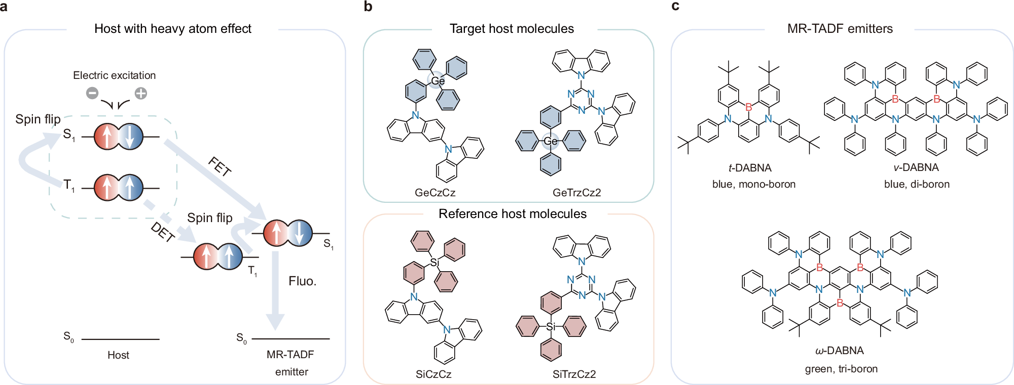
Turning a triplet into a singlet requires an electron spin to flip, and the force that flips a spin comes from spin-orbit coupling. Spin-orbit coupling grows stronger with atomic number. This much is textbook.
So the solution to date has been to attach heavy atoms to the emitter molecule itself. Building them into the skeleton or hanging them off the periphery has pushed reverse intersystem crossing rates above 106 s-1, and green devices have recorded external quantum efficiencies of 36.8%.
Two inconveniences come with it.
First, it has to be designed anew for every emitter. In the paper’s phrasing, it is a case-by-case response. A heavy-atom design made for blue does not carry over as is to a green molecule. That means a materials maker with emitter assets already in hand has to synthesize them again.
Second, the other detour, the exciplex host route, complicates deposition. Mixing a hole transport material and an electron transport material to form an exciplex, then adding a TADF sensitizer and a terminal fluorophore, means depositing four independent components at once. The demands on the deposition equipment rise accordingly.
The group’s framing starts here. If the heavy atom goes into the host rather than the emitter, could the same effect be had without changing the emitter? If so, one host becomes a general strategy applicable across many emitters.
2. Silicon to germanium
The starting point is a pair of already known triphenylsilyl hosts. The hole transporting SiCzCz and the electron transporting SiTrzCz2 form an exciplex when mixed in equal proportion.
From there the group synthesized GeCzCz and GeTrzCz2 by changing only silicon (atomic number 14) to germanium (atomic number 32), obtained by Buchwald-Hartwig and Suzuki-Miyaura reactions respectively.
What makes this substitution a good experiment is the things that did not change.
| Item | Silicon host | Germanium host |
|---|---|---|
| triplet energy T1 | around 2.94 / 2.91 eV | 2.94 eV (GeCzCz) · 2.91 eV (GeTrzCz2) |
| exciplex emission wavelength | around 470nm | 470nm |
| HOMO and LUMO spatial separation | holes on the biscarbazole, electrons on the triazine | identical |
| bond length | C-Si about 1.88Å | C-Ge about 1.95Å |
Triplet energy staying put means the degree to which energy leaks back from emitter to host is unchanged, and the maintained spatial separation of HOMO and LUMO means the electronic structure itself was not touched. In other words, if device performance changes, the cause can be narrowed to the heavy-atom effect alone.
The spin-orbit coupling matrix elements confirmed by calculation are as follows.
| Item | Silicon exciplex | Germanium exciplex |
|---|---|---|
| ⟨S1|ĤSOC|T1⟩ | 0.265 cm-1 | 0.791 cm-1 |
| ⟨S1|ĤSOC|T2⟩ | 0.080 cm-1 | 0.174 cm-1 |
About a threefold rise. Raising the atomic number from 14 to 32 shows up directly.
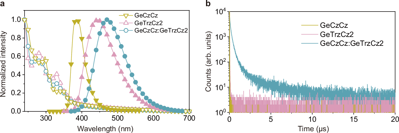
The photophysics of the host exciplex itself improved along with it.
| Item | Silicon | Germanium | Change |
|---|---|---|---|
| singlet radiative decay rate kr,S | 2.5×10⁶ s-1 | up by a factor of 1.9 | |
| singlet non-radiative decay knr,S | 2.1×10⁶ s-1 | down by a factor of 1.5 | |
| photoluminescence quantum yield | 30% | 54% | factor of 1.8 |
| reverse intersystem crossing rate kRISC | 8.0×10⁵ s-1 | up by a factor of 1.3 | |
| delayed fluorescence lifetime | 1.9μs | 1.6μs | |
| prompt fluorescence lifetime | 186.8ns | 173.0ns |
For the drop in non-radiative decay the group points to the denser molecular packing germanium produces. Single-crystal X-ray diffraction gave a higher crystal density for the germanium compound than for the silicon one, which they read as the result of stronger dispersion interactions between molecules.
3. Blocking Dexter, keeping Förster
The host getting better and the host getting better once an emitter is in it are separate matters. The group checked this by doping in three MR-TADF emitters differing in boron count, each at one weight percent: t-DABNA with a single boron (deep blue), υ-DABNA with two (blue) and ω-DABNA with three (green).
This is where the paper’s second point arrives. There are two paths by which energy crosses from host to emitter, and the germanium host picked out just one of them to block.
Förster transfer is the path that hands singlet energy across at a distance; Dexter transfer is the path that exchanges electrons directly and carries triplets across too. Once a triplet has crossed to the emitter it is stuck there, because the slow reverse intersystem crossing of MR-TADF emitters was the problem in the first place.
| Emitter | Förster radius | Dexter transfer rate | Delayed fluorescence lifetime | Reverse intersystem crossing rate |
|---|---|---|---|---|
| t-DABNA (deep blue) | 4.7nm | down by a factor of 1.33 | shortened by a factor of 1.18 | up by a factor of 1.69 |
| υ-DABNA (blue) | 7.6nm | down by a factor of 1.70 | shortened by a factor of 1.67 | up by a factor of 2.02 |
| ω-DABNA (green) | 8.5nm | down by a factor of 3.05 | shortened by a factor of 2.14 | up by a factor of 2.08 |
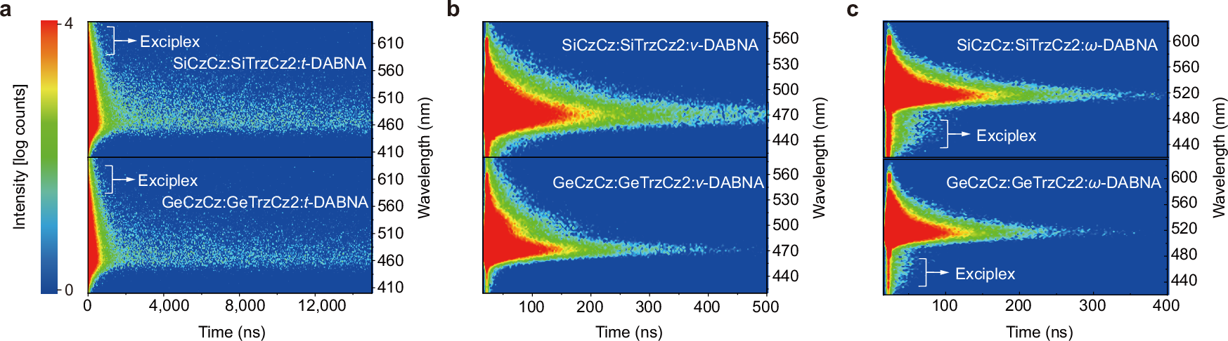
The larger the emitter’s Förster radius, the larger the improvement. As the host’s singlet energy crosses reliably to the emitter, triplets stay on the host side and are turned back by the accelerated reverse intersystem crossing. The reverse intersystem crossing rate of υ-DABNA reached 9.1×10⁵ s-1.
4. Device results
The devices stack, on indium tin oxide, HAT-CN 5nm, TAPC 30nm, TCTA 15nm, GeCzCz 15nm, emissive layer 25nm, GeTrzCz2 20nm, ANT-BIZ 30nm, Liq 2nm and aluminium 100nm. The emissive layer holds the two hosts and the dopant at a weight ratio of 0.50 to 0.49 to 0.01.
The controls are the same structure with only the host changed to silicon (SiCzCz:SiTrzCz2) or carbon (CCzCz:CTrzCz2).
External quantum efficiency
| Device | Peak EQE | 1,000 cd/m2 | 5,000 cd/m2 |
|---|---|---|---|
| υ-DABNA · germanium | 40.1% | 32.8% | 24.4% |
| υ-DABNA · silicon | 34.1% | 22.4% | 14.6% |
| υ-DABNA · carbon | 36.7% | 19.7% | 3.2% |
| ω-DABNA · germanium | 40.4% | 33.4% | 23.9% |
| ω-DABNA · silicon | 35.3% | 24.7% | 10.5% |
| ω-DABNA · carbon | 33.0% | 21.7% | 9.9% |
| t-DABNA · germanium | 30.1% | 12.0% | 7.6% |
| t-DABNA · silicon | 26.9% | 7.5% | 4.5% |
| t-DABNA · carbon | 16.8% | 2.5% |
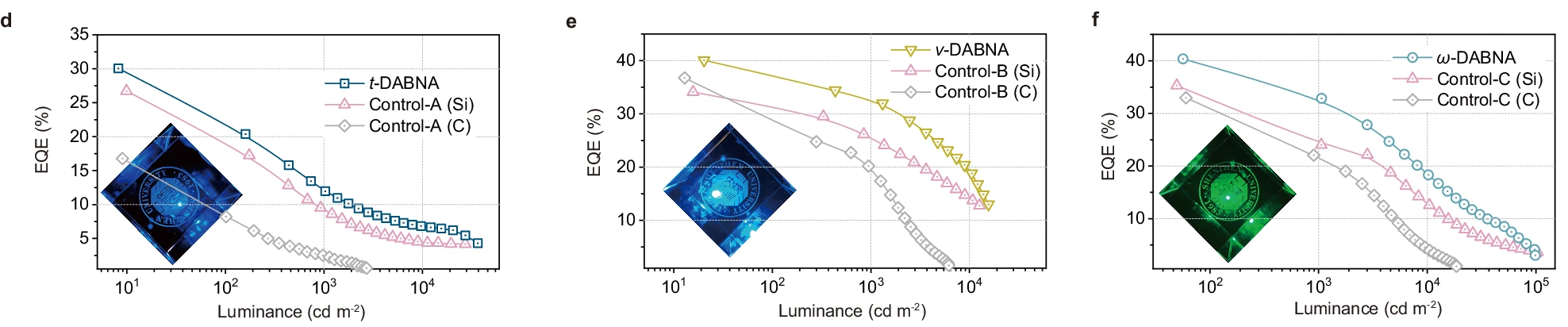
The heart of this table is that the gap widens as brightness rises. Look only at peak efficiency and the difference between the germanium and carbon hosts for υ-DABNA is 40.1% against 36.7%, hardly large. At 5,000 nits it becomes 24.4% against 3.2%. What suppressing efficiency roll-off actually means lies between those two numbers.
Put as the efficiency drop at 1,000 nits, it reads as follows.
| Emitter | Germanium | Silicon | Carbon |
|---|---|---|---|
| υ-DABNA | 18.2% | 34.3% | 46.3% |
| ω-DABNA | 17.3% | 30.0% | 34.2% |
Reproducibility of the efficiency itself was also checked. Averages over twenty devices were 39.2±0.9% for υ-DABNA and 39.3±0.7% for ω-DABNA.
Spin dynamics, not optics
The possibility that the high efficiency owed to emitting dipole orientation was checked separately and ruled out. The horizontal emitting dipole ratios of the three hosts are effectively the same: 89.1±2.0% (germanium), 88.2±1.7% (silicon) and 88.0±1.7% (carbon). Theoretical maximum efficiencies from optical simulation were also nearly identical across the three hosts.
And yet only the germanium host devices came close to the theoretical value. That the optical conditions are the same while the measurements diverge means the difference arose not at the stage of extracting light but at the stage of turning triplets back into singlets.
Colour coordinates and lifetime
| Device | Emission peak | CIE coordinates |
|---|---|---|
| t-DABNA | 460nm | (0.154, 0.141) |
| υ-DABNA | 469nm | (0.125, 0.113) |
| ω-DABNA | green | (0.154, 0.741) |
The green device’s coordinates sit close to the Rec. 2020 green reference (0.170, 0.797). The group states that the υ-DABNA and ω-DABNA devices exceeded the previous best efficiencies in the blue region below CIEy 0.20 and the green region above 0.71 respectively, a comparison that includes platinum phosphorescent devices and TADF-sensitized routes.
Half-lives (LT50) measured at an initial luminance of 1,000 nits are as follows.
| Emitter | Germanium | Silicon | Carbon |
|---|---|---|---|
| t-DABNA | 8.8 hours | 9.0 hours | 0.2 to 0.5 hours |
| υ-DABNA | 29.3 hours | 24.6 hours | 0.2 to 0.5 hours |
| ω-DABNA | 241.1 hours | 207.8 hours | 0.2 to 0.5 hours |
Why the carbon host dies so quickly is explained by transient electroluminescence measurements. Taking υ-DABNA as the reference, the lifetime of the delayed component came out at 95.60μs for carbon, 67.30μs for silicon and 34.20μs for germanium. The relation that the more long-lived triplets accumulate, the faster the device ages shows through directly. The electrochemical stability of the three hosts came out similar in cyclic voltammetry, so the lifetime difference cannot be explained by the materials’ resistance to oxidation and reduction.
With t-DABNA, on the other hand, germanium and silicon were effectively the same at 8.8 hours against 9.0 hours. The group attributes this to the high emission energy of t-DABNA putting the chemical stability of both hosts on trial. That this device’s efficiency stopped at 12.0% at 1,000 nits is likewise down to incomplete Förster transfer from host to t-DABNA. It follows from the earlier table, where its Förster radius of 4.7nm was the shortest of the three.
5. What it means
The value of this paper for display materials lies less in the efficiency figures than in how it is applied.
First, the emitter does not have to be resynthesized. Because the heavy-atom effect is obtained in the host rather than the emitter, an already validated emitter can be left alone and only the host swapped. The paper indeed applied the same host to three emitters differing in boron count and confirmed improvement in all of them. A materials maker’s accumulated emitter assets stay alive.
Second, the number of deposited components falls. The established route of adding a TADF sensitizer to an exciplex host demands four-component co-deposition. This structure has three: two hosts and one dopant. Energy passes straight from host to emitter without an intermediate sensitizing step.
Third, the condition is clear. Where this strategy works well is with emitters whose Förster radius is large enough. Across the three emitters the Dexter suppression (factors of 1.33, 1.70 and 3.05) and the radius (4.7nm, 7.6nm and 8.5nm) grew together, and the improvement in device performance followed the same order. For anyone evaluating a new host, that becomes a practical guideline: look first at the overlap between the emitter’s absorption spectrum and the host’s emission spectrum.
Two things to add at the end. The author list contains two researchers from Wuhan China Star Optoelectronics Semiconductor Display (TCL CSOT). And Shenzhen University states in the paper’s competing interests section that it has filed a Chinese patent on the materials and devices (application number 2024117894081), now under examination. Worth reading as a signal that this was not research undertaken with the intention of stopping at the academic stage.
Sources
- Zhang, X., Chen, Z., Huang, M. et al. Germanium-integrated exciplex host for high-performance narrowband OLEDs with mitigated efficiency roll-off. Nature Communications (2026). Published online 2026-08-20. DOI 10.1038/s41467-026-76914-5 · CC BY 4.0
- Every figure in the text is a value confirmed directly in the body, Table 1 and supplementary descriptions of that paper. Device performance figures are cited from the same row for each device, with no mixing of best values obtained under different conditions.