How does the screen turn itself off during a call?
Pass a proximity sensor signal through an OLED twice and its strength falls as the square of the transmittance (T²). Raise the emission to secure signal margin and a reliability risk follows: TFT photodegradation. How an engineer designing under-display sensors should resolve that trade-off.
This article was published before the English edition began, so the labels inside its figures and simulators are in Korean. The caption and the note under each figure are in English.
1. When a hand comes near the screen
A call comes in, and the moment an ear goes to the screen it turns off. Behind that familiar behaviour is a chip smaller than a fingernail, hidden beneath the OLED panel. The proximity sensor. Where the UDC camera of the previous episode was a problem of “forming an image from light coming in from outside,” the proximity sensor is a problem of “the panel firing light itself and receiving the reflection back.”
This chip’s task is simple. Is something close in front of the screen right now? But the way it finds the answer is the opposite of passive sensing. It cannot judge by quietly receiving light coming from outside. A proximity sensor has to fire light itself and check directly whether that light comes back. And in near-infrared invisible to the human eye, at a wavelength of 940nm.
Why go to the trouble of firing invisible light? Visible light is already full of ambient lighting and sunlight, so the sensor cannot distinguish the light it fired from the light that was already there. Near-infrared at 940nm, by contrast, is a “clean” band barely mixed into natural light, so whether the light returning now is the light just fired can be told clearly.
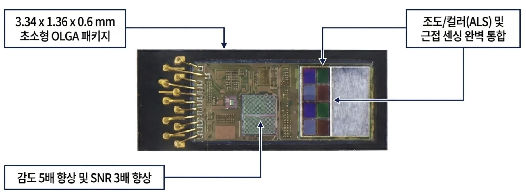
Thanks to this active sensing, the screen not only turns off automatically during a call but can also tell whether a cover case has closed over it or it has gone into a pocket. The problem is that this “fire and receive” method sets the OLED panel an entirely new piece of homework.
2. Why the signal disappears as a square
Near-infrared passes through the panel twice. Once going out, once returning after reflecting off an object. Call the panel’s IR transmittance T and the final signal falls in proportion to T². According to patent US12050264, the IR transmittance of an OLED panel is roughly 3 to 10%, and squaring that value drops the actual received signal to 0.09 to 1%.1 It is weaker by orders of magnitude than sensing that passes light only once. Most of the loss occurs in the metal cathode layer; the polarizer in fact passes IR well and is not the culprit.
Another variable enters here: the light-blocking layer (BML) covered in the next section. The thicker the blocking layer is made to protect the TFT, the more it also blocks the very IR that must pass. Below you can move the blocking ratio and the panel aperture transmittance yourself and see this trade-off.
3. The TFT is threatened in a new way
Once a light source exists, the TFT is threatened in a new way. LTPS and oxide (IGZO) TFTs respond to light by nature, so OLED panels carry, from the design stage, a light-blocking structure against external light entering from the front. But a structure designed to block frontal light cannot block the exposure path of an IR source newly created at the panel’s rear. So a separate bottom metal layer (BML) has to be added beneath the driving TFT (T1).2
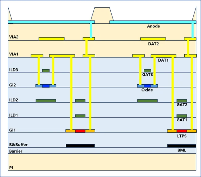
Why is T1 (the driving TFT) especially vulnerable? T1 is the device directly controlling the current flowing into the OLED. Under IR irradiation a photocurrent arises in the active layer, shifting the threshold voltage (Vth). A shifted Vth makes T1 pass more or less current than set, producing an error in OLED luminance. The result is the screen blotch appearing in the IR-irradiated region, the so-called watermark artifact.3 LTPS (polycrystalline silicon) and oxide (IGZO) are vulnerable by different paths. LTPS has a narrow bandgap of about 1.1eV, so photocurrent can increase even in the 850 to 940nm band via grain boundary trap states, while IGZO is by nature more sensitive to ultraviolet and visible light but was recently confirmed in IGZO phototransistor research to give a substantial photoresponse even near 850nm through surface oxygen defect levels (responsivity 42.5A/W).4
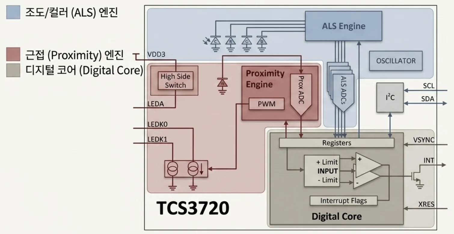
ams’s TCS3720 is a 3-in-1 sensor integrating an ALS engine and a proximity engine on one die. An LED drive pin turns on the IR LED, and the reflected wave becomes a digital signal through analogue-to-digital conversion. The key is the VSYNC pin. It takes the display frame signal and fires and receives IR only during the blanking interval.
4. Other challenges
A new demand is laid on the BPDL (black photo-definable layer) and BM (black matrix) that partition the pixels too. These blocking films, which originally raise contrast by stopping light leaking between pixels, do their job only by being completely opaque to visible light. In the proximity sensor era, one more contradictory demand is laid on the same material: that it pass 940nm near-infrared alone. It needs dual optical properties, jet black to the human eye and transparent in the IR wavelength window.
Materials with these dual properties already exist. Patent US20160200912A1 presents a light-blocking pigment composition for displays securing transmittance below 1% in the visible (400 to 800nm) and above 80% in the near-infrared (800 to 1100nm).5 The key is using perylene-family pigments instead of carbon black, and a patent published in 2025 (WO2025031982A1) covers a formulation further improving the near-infrared transmission of these perylene black pigments.6 The same principle exists in the automotive industry. To hide lidar and camera sensors under body paint, pigments looking “black to the eye, transparent to the sensor,” such as DIC’s Spectrasense™ family and BASF’s PALIOGEN® Black family, are already commercialized.7 Below you can change the material and see how the visible and IR transmission spectra differ.
Another direction is to do away with the separate chip altogether. Organic photodiodes (OPD) can respond to near-infrared. Add a self-emitting and light-receiving integrated device that also emits, and a structure where the pixel itself is both emitter and receiver becomes possible. It is still at the crawling stage, but a research theme by which a panel company can differentiate.
5. Questions remaining
① Blocking and transmission: how far to compromise
Cover T1 completely and photodegradation disappears, but the IR transmittance falls with it. Rather than lowering a transmittance already only 3 to 10%, layout optimization — covering only T1’s position selectively, or using the pixel apertures and inter-pixel gaps as the IR path — is under discussion as the realistic compromise. What the optimal blocking ratio is has no published quantitative standard yet.
② Can crosstalk be eliminated entirely?
Directly coupled light that never reaches the object but scatters and reflects inside the panel and leaks straight into the receiver is noise indistinguishable from the reflected wave. It can be reduced by physically separating emitter and receiver or raising an optical barrier, but the thinner the panel gets, the less of that spare room there is.
6. Key terms
- proximity sensor
- An active sensor judging whether an object is close to the screen by firing light itself and receiving the reflected wave.
- T²
- The transmittance loss near-infrared suffers on its round trip (transmit plus receive) through the panel. The signal falls in proportion to the square of the one-way transmittance T.
- BML
- Bottom metal layer. A metal blocking layer added at the bottom of the stack to protect the driving TFT (T1) from rear-side IR.
- watermark artifact
- A local luminance error arising when IR irradiation shifts the TFT threshold voltage. It appears on the screen as a blotch.
- BPDL/BM
- Blocking films stopping light leaking between pixels. For proximity sensing they are required to have dual properties, blocking visible light while passing IR alone.
Footnotes
-
Patent US12050264. The OLED panel near-infrared transmittance of 3 to 10% and the bidirectional emit-receive structure are its grounds. ↩
-
Patents US9666120 (a blocking structure preventing driving TFT photodegradation) and US11978396 (a dual blocking layer structure). ↩
-
Patent US10984731. It covers the brightness anomaly (flicker and blotching) arising from interaction between the IR emitter and the pixel circuit in an under-display sensor region, and structures easing it. ↩
-
Research on 850nm near-infrared detection in IGZO phototransistors. It reports achieving a responsivity of 42.5 A/W and an external quantum efficiency of 6.2×10³% using interfacial oxygen defects. ↩
-
Patent US20160200912A1. It specifies that the light-blocking pigment composition for displays satisfies both transmittance below 1% in the visible (400 to 800nm) and above 80% in the near-infrared (800 to 1100nm). ↩
-
Patent WO2025031982A1 (published 2025). It covers a formulation improving the near-infrared transmission of perylene black pigments. ↩
-
Published product material for DIC Spectrasense™ Black L 0082 and the BASF PALIOGEN® Black family. Not for displays, but commercial pigments on the same principle, hiding automotive lidar and camera sensors black to visible light and transparent at the sensor wavelength. ↩