Why does a selfie shot through the screen come out fine?
UDC image degradation is the price of lowering pixel density, and a single phenomenon, diffraction, creates three defects at once: blur, flare and halo. The solutions split two ways, computational restoration (software) and metasurfaces (optics). From principle to patent landscape, for the optical and pixel design engineers who have to decide which one to invest in.
This article was published before the English edition began, so the labels inside its figures and simulators are in Korean. The caption and the note under each figure are in English.
1. How the hole-less screen came about
The other sensors hidden under an OLED, the ambient light sensor and the proximity sensor, were a matter of “does light pass through.” The ambient light sensor only had to measure one quantity of light, the proximity sensor only had to send one signal there and back. UDC is different. It has to form an image of millions of pixels from the light that got through. Passing through is not enough; it has to be sharp.
The Axon 20 that ZTE put out in September 2020 had no camera hole anywhere on its screen. It was the world’s first commercialized under-display camera, and the trick was simple: the pixels where the camera sat were arranged more sparsely than the rest. That was all.
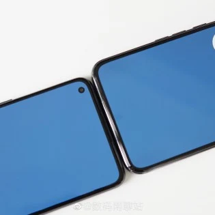
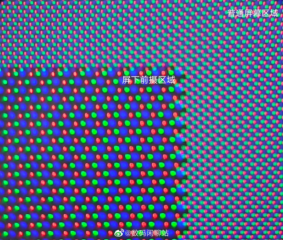
A punch-hole phone (left) and the ZTE Axon 20 (right). There is no hole on the right. Source: GSMArena Macro shot. The camera region on the left has sparser pixels than the ordinary screen on the right. Source: GSMArena
Competition over this position is still under way. Visionox filed first on a dual low-density and high-density structure, and BOE refined it a step further into a chequerboard arrangement. Other panel makers including Samsung have each accumulated patents on variant structures. The goal of hiding a camera under the screen is the same while the arrangement differs by company, and those minute differences became the boundary line of disputes. In 2026 BOE filed a patent infringement suit against Samsung in a US court.1
Table 1 · Comparison of pixel arrangements in the camera region
| Party | Arrangement | Aim | Timing |
|---|---|---|---|
| ZTE Axon 20 | low density only in the camera region | first commercialization. transmittance takes priority | 2020.09 |
| Visionox | dual low-density and high-density structure | eases the visible brightness step at the boundary | earlier filing |
| BOE | chequerboard (grid alternating) arrangement | distributes the transmitting sections to ease diffraction fringes | improvement |
| Samsung and others | numerous variant arrangements | design-around. the target of BOE’s 2026 suit | 2026 dispute |
Source: compiled from each company’s published patents and publicly known litigation facts. Interpretation of claim scope is not included.
2. Why the image quality worsens
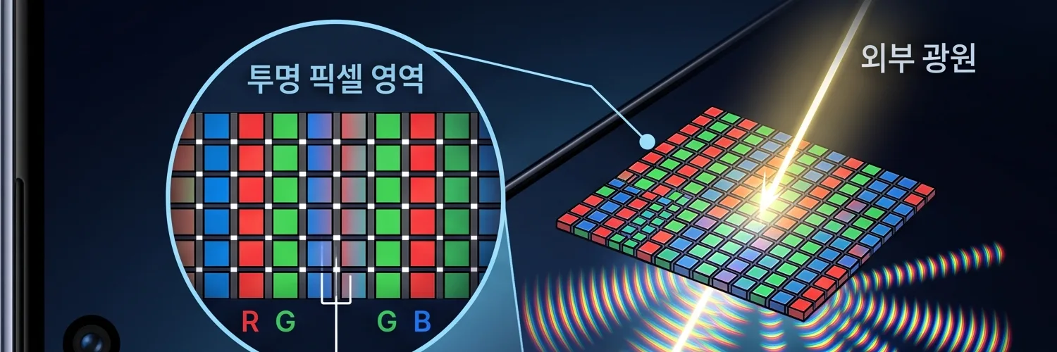
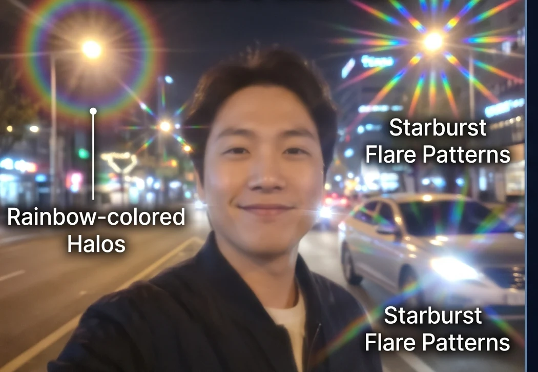
The screen above the camera is not thinned out at random. Transparent gaps open between the pixels in a regular pattern. The problem starts here. Light is a wave, and a wave passing through narrow gaps repeating regularly does not travel straight. It spreads in all directions, interferes with itself and makes fringes. Diffraction. The same principle by which a streetlight seen through a fine insect screen appears smeared enters every image an under-screen camera receives.
The lower the density, the more light comes in. But at the same time that regularly thinned arrangement itself increases the diffraction. The more you open it, the blurrier it gets — that is the paradox. The fundamental trade-off UDC design is held by is here.
You can move the gap width and the wavelength yourself and see how the diffraction angle changes.
Table 2 · The three image degradations diffraction makes
| Phenomenon | What is seen | Physical cause |
|---|---|---|
blur Blur | sharpness falls across the whole image | light from one point spreads out broadly instead of forming a sharp point |
flare Flare | star-shaped streaks extend from a bright light source | the spread light aligns along the grain of the grid |
halo Halo | a rainbow rim around a light source | the bending angle differs by wavelength, so colours separate |
3. Filling it in by calculation: restoration algorithms
Diffraction that structure could not fully block has to be filled in somewhere. Since the ECCV challenge of 2020, the computer vision field has held a competition on this problem every year. An actual UDC panel is placed in front of a camera, a monitor is photographed to measure the point spread function (PSF) — how far a single point source spreads when captured — and that data is used to restore the blurred image in reverse.
Google solved the same problem differently. It divided the camera region into two sections and planted a light-blocking pattern of a different shape in each. One is rectangular, the other circular. Under the rectangular pattern is a monochrome sensor, under the circular one a colour sensor. One yields an image favourable to sharpness and the other one favourable to colour reproduction, and the two are then merged by artificial intelligence.2
Rather than striving to remove the distortion, deliberately design two different distortions, extract two kinds of information, and build one image by calculation.
4. Erasing it optically: metasurfaces
In 2025 a route appeared that needs no calculation at all: the metasurface, an optical surface designed at the nanometre scale. It optically suppresses the higher-order diffraction modes made by the regular pixel arrangement, obtaining a clean image in real time without passing through a neural network. It is the approach of erasing the cause itself optically rather than correcting after the fact.3
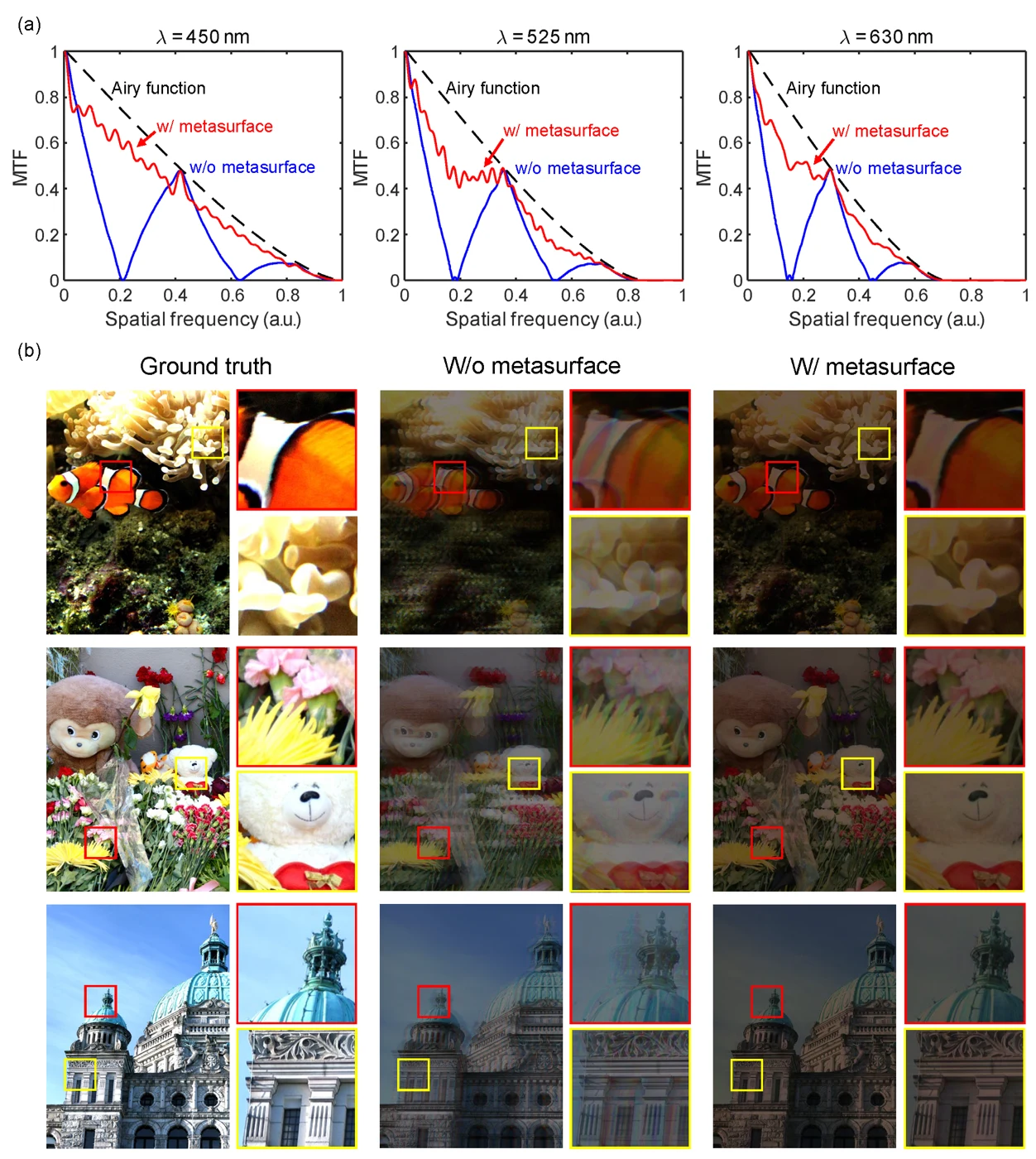
You can move the suppression strength yourself and see how close the measured MTF curve comes to the ideal Airy curve.
Table 3 · The two branches of solution compared
| Category | Software · restoration algorithm | Hardware · metasurface |
|---|---|---|
| Point of intervention | after capture (undoing the blurred image) | before capture (suppressing the diffraction itself) |
| Maturity | a conference challenge every year since 2020. an established field | at the 2025 paper stage. before production validation |
| Cost | compute resources and latency | an added nanostructure process |
| Limit | there is a limit to restoring lost information | covering the whole visible band at once is the challenge |
5. Two questions remaining
① The metasurface is still before production validation
Designing a nanostructure to suppress diffraction across the whole visible band (450 to 630nm) at once, and being able to lay that structure onto an existing OLED panel process as it is, are different problems. Whether paper-level performance reproduces on an actual production line is not yet confirmed.
② Optics and calculation: where to draw the line
Filling in by calculation and suppressing optically are less a competitive relation than a combinable one. Optimizing the division of roles — how far the panel structure blocks and from where the neural network restores — is the substantive design problem of the next stage.
6. Key terms
- UDC
- Under-display camera. A structure placing the camera beneath the screen to remove the front-face hole.
- diffraction
- The phenomenon in which a wave passing regular narrow gaps spreads and interferes to make fringes. The single cause of UDC image degradation.
- PSF
- Point spread function. A function expressing how far a single point source spreads when captured, and the input to restoration algorithms.
- MTF
- Modulation transfer function. A sharpness indicator expressing how much contrast is preserved at each spatial frequency.
- metasurface
- An optical surface controlling the phase and amplitude of light by arraying nanostructures smaller than the wavelength.
Footnotes
-
The patent infringement suit BOE filed against Samsung in a US court in 2026. The text covers only the fact of the filing and carries no judgement on claim scope or infringement. ↩
-
Google patent EP4218225A1. A structure combining two light-blocking patterns and two kinds of sensor and then fusing them by machine learning. ↩
-
arXiv:2504.17368. Research suppressing higher-order diffraction modes with a metasurface. At the paper stage; application to a production process is not validated. ↩