
Sensing, memory and computation in a single flexible transistor
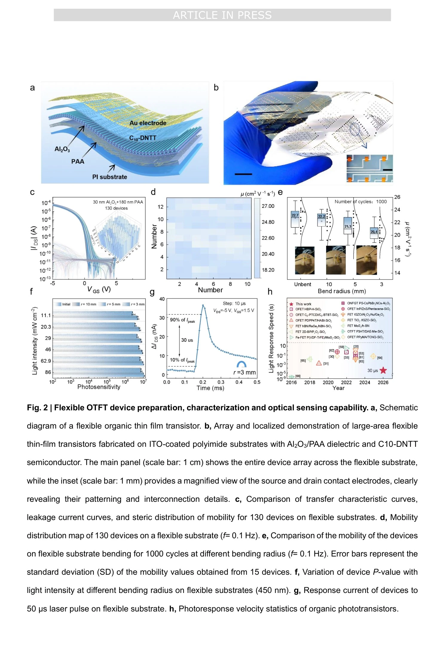
Merge three devices — sensor, memory and processor — into one and the component count and wiring fall accordingly. A flexible OTFT with inorganic-organic heterogeneous dielectrics secures a mobility of 22.65cm²/V·s and a photoresponse of 30 microseconds at the same time, showing that device integration is possible without loss of performance. Worth a look for teams designing flexible electronics modules.
DOI 10.1038/s41467-026-76116-zArtificial vision systems have so far made and joined separate devices for detecting light, storing information and computing. A joint team from Tianjin University, Nanjing University of Posts and Telecommunications and Jilin University crammed all three into one transistor. On a flexible substrate it takes 30 microseconds to detect light, and holds that information for more than 10 years.
1. Why this was a hard problem
Devices exchanging signals with light have lagged uniquely far behind. Integrated devices driven by electrical pulses already have nanosecond speeds, retention above 10 years, endurance above 1 million cycles and recognition accuracy above 95%, while the optically pulsed devices essential to visual sensing remained at millisecond speeds, retention on the order of 10,000 seconds, endurance under 1000 cycles and recognition accuracy around 90%.
Try to close that gap with organic semiconductors and a new wall appears. Tune the semiconductor for high mobility and fast switching and the memory retention falls below 1000 seconds, effectively volatile; tune the dielectric instead for charge trapping (memory retention) and mobility and speed worsen badly. An interface design capturing mobility and memory retention together was the unsolved homework.
2. The turn: reversing the stacking order
Stacking inorganic and organic materials together usually follows the order “organic on inorganic,” because of the high-temperature process constraints of the inorganic. The group reversed it. Polyamic acid (PAA) was spin coated first, and thin aluminium oxide (Al₂O₃) was grown on top of it by low-temperature (80℃) plasma atomic layer deposition.
The result gains, in one device, both the excellent charge transport the self-aligned nanogroove structure of PAA provides and the deep charge traps (excellent memory retention) made by the oxygen vacancies of Al₂O₃. A memory device was made without sacrificing mobility.
3. Result: it senses, stores, and responds like an eye
Pure response speed to an electrical signal reached 130 nanoseconds, while the stable multi-level programming speed that actually stores an image was 10 microseconds. The two are separate figures measured under different conditions. After 1000 bends at a 3mm radius it retained 90% of its initial mobility.
The device was used to recognize three things: handwritten digits, hand gestures and faces. Flat, the accuracies were 94.78% for digits, 99.83% for gestures and 92.56% for faces, and bent to 3mm they did not fall far, at 93.88%, 96.67% and 91.96% respectively. These figures are not the result of the device inferring directly in real time but values computed by feeding the measured synaptic characteristics of the device into a simulation (NeuroSim).
An actual hardware demonstration was also built. The measured synaptic characteristics of the device were loaded as a weight model onto a Zynq FPGA board, with the convolution operations of a lightweight neural network (YOLOv3-tiny) handled by the FPGA, constituting a real-time face detection system. It did not respond to dolls or mechanical eyes, and picked out only faces accurately even with a mask on or against a background of mixed objects.
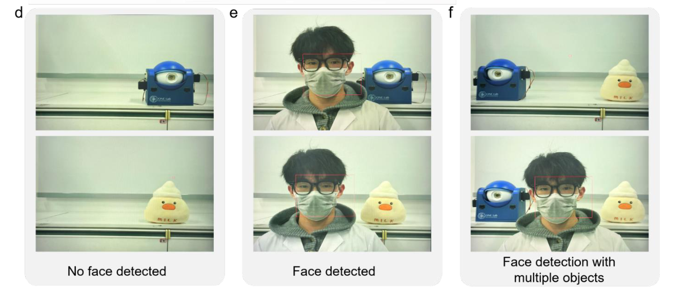
It also imitated the movement of the human eye, whose pupil narrows reflexively under strong light. The device array is placed behind an artificial pupil, and when it detects an optical signal an external circuit closes the pupil with it.
4. What it means: a vision sensor paper, not a display one, and yet
This paper aims from beginning to end at intelligent object detection and edge computing for aerospace. The words “display” and “backplane” do not appear once in its body. So it is hard to see this device as made for displays.
From a materials and process point of view, though, there is something for the display industry to watch. Mobility above 20cm²/V·s on a flexible substrate, compatibility with an 80℃ low-temperature process, and stability retaining 90% at a 3mm bend overlap exactly with the core indicators a flexible AMOLED backplane TFT demands. It is not a device made for displays, but for an engineer wrestling with flexible backplane process it is a low-temperature heterogeneous dielectric result worth consulting.
5. At a glance
| In one line | reversing the stacking order of inorganic-organic heterogeneous dielectrics integrates sensing, memory and computation in one flexible OTFT (mobility 22.65cm²/V·s, photoresponse 30µs) |
| Core results | charge retention over 10 years (extrapolated) · recognition accuracy 92 to 99% (NeuroSim simulation) · 90% mobility retained after a 3mm bend |
| Strengths | compatible with a low-temperature (80℃) process, higher mobility on a flexible substrate than on a rigid one |
| Published | Nature Communications, 2026 (Article in Press) |
6. Key terms
- OTFT
- A thin film transistor using an organic semiconductor as its channel. It allows lower-temperature, lower-cost processes than inorganic semiconductors and suits flexible substrates well.
- inorganic-organic heterogeneous dielectric
- A dielectric structure stacking two different materials (here Al₂O₃ and PAA) to secure at once properties hard to get from either alone (charge transport plus charge trapping).
- retinomorphic
- Meaning modelled on the retina. It refers to reproducing in an electronic device a biological visual reflex such as the pupil narrowing immediately in response to light.
- NeuroSim
- A simulation tool that takes synaptic characteristics measured on a real device (conductance change and so on) as input and computes how a neural network would perform if built from that device.
The other 9 papers of the week are swept briefly in the display paper briefing for week 4 of July.