
Mobility and stability of an oxide TFT, both held by fluorine
The trade-off where raising mobility collapses stability, solved for both by adding a single ion implantation step to the IGZO TFT channel. With boron difluoride (BF₂) implantation, mobility rises from 12.1 to 35.8cm²/V·s while the threshold voltage shift improves from 2.46 to 1.74V. It means specifications can be raised together without adding process steps, a result for anyone working on backplane process.
DOI 10.1002/adfm.77185Oxide semiconductor TFTs have carried an old dilemma. Raise the mobility and stability falls; grip the stability and the process gets complicated. A Yonsei University group held both together merely by planting one ion in the channel. Under boron difluoride implantation, mobility jumped from 12.1 to 35.8cm²/V·s, close to threefold, while the threshold voltage shift under the same condition actually fell.
1. Why this was a hard problem
Oxide semiconductor TFTs such as IGZO have lower mobility than LTPS TFTs and are especially vulnerable to threshold voltage drift under long operation, high temperature and light exposure. Accumulated electrons create defects inside the amorphous oxide, and under light the oxygen vacancies (V_O) ionize and the charge balance is disturbed.
Responses so far have changed the IGZO composition, added passivation and light-blocking layers, or compensated at the circuit level. But most of these approaches added process steps while recreating the very trade-off between performance and reliability. Ion implantation itself is already in use, but until now only to lower the contact resistance of the source and drain regions; cases applying it to the channel region itself were rare.
2. The turn: the same place, a different ion
The group implanted boron (B) or boron difluoride (BF₂) ions directly into the IGZO channel through a screen oxide (HfOx). The dose was held identical at 1×10¹⁵ ions/cm², with only the ion species and energy changed.
Implanting boron alone increased oxygen vacancies and oxygen interstitial defects together, so mobility rose but stability actually worsened. With boron difluoride, on the other hand, the fluorine ions passivate the oxygen vacancies, keeping the mobility gain while improving stability as well. Doping and defect control were achieved at once by a single ion implantation step, with no multi-step process adding a separate doping or passivation layer.
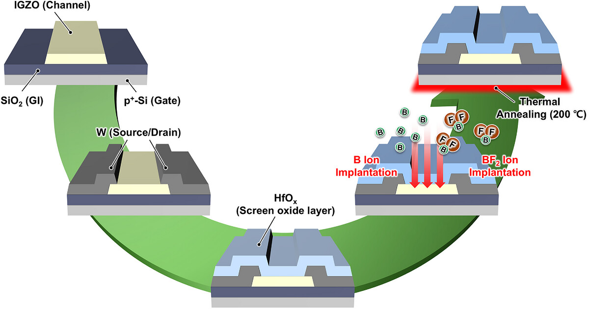
3. Result: where boron and fluorine part
Table 1 · Performance before and after implantation (dose identical at 1×10¹⁵ ions/cm² for all conditions)
| Condition | Mobility [cm²/V·s] | PBTS ΔVth [V] | NBIS ΔVth [V] |
|---|---|---|---|
| pristine | 12.1 | 2.46 | 3.12 |
| B, 40 keV | 37.2 | 4.44 (worse) | 4.39 (worse) |
| BF₂, 40 keV | 35.8 | 1.74 (better) | 1.04 (better) |
| B, 60 keV | 38.6 (highest mobility) | 7.72 | 6.22 |
PBTS: +20V gate voltage, 60℃, 10,000 seconds of stress. NBIS: −20V gate voltage with white light (5700lux) illumination, 10,000 seconds. With boron, the higher the energy the higher the mobility but the worse the stability. Boron difluoride goes the other way. Source: paper Table 1, Figures 3 and 4.
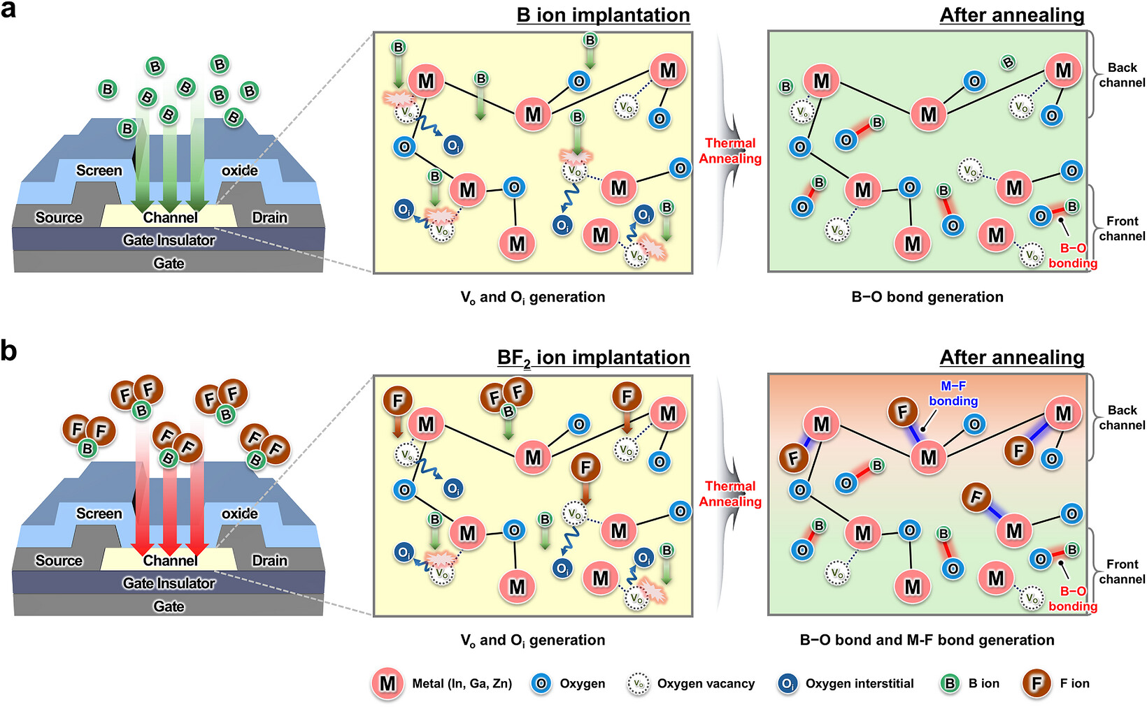
4. What it means: one new variable in backplane process
IGZO TFTs are already the core material of this generation’s premium display backplanes. That mobility and stability improve together without adding process steps also means the existing ion implantation infrastructure (for source and drain doping) can be extended as it is into the channel process.
This result is at test device scale (channel width and length 100µm), though, and the stress testing went only as far as an accelerated test of 10,000 seconds (about 2.8 hours). Uniformity and yield data in a large-area panel process are not yet available.
5. At a glance
| In one line | implanting BF₂ ions directly into the IGZO channel improves mobility (12.1→35.8cm²/V·s) and stability (PBTS ΔVth 2.46→1.74V) at once |
| Core results | at BF₂ 40keV, mobility 35.8cm²/V·s · PBTS ΔVth 1.74V · NBIS ΔVth 1.04V (the highest mobility of 38.6 is the B 60keV condition, but stability worsens to ΔVth 7.72V) |
| Strengths | doping and defect passivation achieved together by a single ion implantation step, with no separate doping or passivation layer |
| Published | Advanced Functional Materials, 2026 (Early View) |
6. Key terms
- IGZO
- An oxide semiconductor of indium, gallium, zinc and oxygen. Lower in mobility than LTPS but good in large-area uniformity, widely used in high-resolution display backplanes.
- oxygen vacancy (V_O)
- A site in an oxide crystal from which an oxygen atom is missing. It acts like a charge-releasing donor and raises mobility, but in excess also acts as a defect harming stability.
- PBTS / NBIS
- Positive bias plus thermal stress, and negative bias plus illumination stress, respectively. Standard stability tests measuring how far the threshold voltage drifts when a TFT is on for a long time or exposed to light.
- channel ion implantation
- A process forcing particular ions into a semiconductor. Previously used only to lower source and drain resistance; cases applying it to the channel itself were rare.
The other 21 papers of the week are swept briefly in the display paper briefing for week 3 of July.